Facebook
 Google
 GitHub
 Linkedin
Thermal Co-Design, Cooling Architecture Optimization, and Reliability Validation
Explore electro-thermal cooling design and reliability validation for high-voltage SiC and IGBT power modules.
In the introductory article on building electro-thermal models for power modules, we explored the foundation of accurately modelling the behaviour of junction temperature in high voltage 4-6.5 kV IGBT and SiC power modules.
By changing conduction and switching losses into transient thermal responses using Cauer and Foster thermal impedance networks, we show how engineers can manage and predict the behavior of temperature in semiconductors at the device level.
In this second part, we extend our focus from the semiconductor die to the overall system-level thermal path in which substrate interfaces, busbars, and cooling architecture play essential roles in temperature increase and long-term reliability of power systems.
In this case, we are going to analyze the thermal resistance of laminated busbars, and using CFD-supported techniques and analytical methods, compare plate and liquid-based systems to size the cooling system for lifetime-oriented reliability validation correctly.
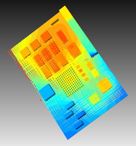
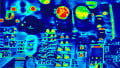
Figure 1. Simulation image of thermal heatmap showing cooling air flow on PCB. Image used courtesy of Wikimedia.
Thermal Modelling of High-Voltage Busbars
Laminated busbars in 4-6.5 kV converter systems form part of active thermal components that, under fast switching and high current density, can become unexpected heat sources that directly influence the semiconductor junction margin, insulation lifetime, and reliability in the long term.
Through multiple coupled electrical phenomena, HV laminated busbars generate heat in various ways, not just through ohmic resistance. This heat is generated through AC losses as a result of proximity and skin effect, DC conduction loss, and heating of the dielectric. When the switching frequency ranges from 2 to 20 kHz, the losses resulting from AC power cannot be neglected.
In such a case, the concentration of current shifts into high-density zones near close conductors in a proximity effect, penning effect, and skin effect as it concentrates towards the surface of the busbars. In laminated copper insulation featured in fast SiC-based switching converters, these phenomena increase the effective AC resistance by up to three times.
Analytical Thermal Resistance Estimation
Before committing to using multiphysics or 3D CAD simulation, analytical thermal resistance can be estimated in laminated busbars, based on the steady-state heat production and simplified convection from the outer surface.
This estimation depends on the heat transfer through convection based on the coolant or air flow represented by the coefficient (h), and the total heat-dissipating surface area (A) of the copper. The temperature change is then estimated by dividing the resistive heating from the flow of current by the product of the surface area and the heat transfer coefficient (k).
$$R_{\theta ,total} = R_{\theta ,cond}~+~R_{\theta ,conv} $$
Where:
$$R_{\theta ,cond} = \frac{t_{Cu}}{k_{Cu}~\times~A_{cond}} ~~ \text{,}~~ R_{\theta ,conv} = \frac{1}{h~\times~A_{surf}}$$
With the equation, copper busbars are considered as a consistent heat source releasing energy only through convection. One of the assumptions on this is that heat is spread evenly and is dissipated uniformly, which goes against the behaviours of the actual laminated busbars. The model can therefore be refined by splitting the total thermal resistance into convection and conduction components. This is essential to account for geometric influences such as copper thickness (tCu) and its thermal conductivity.
$$\Delta T = I^2 \times R_{dc} (R_{\theta ,cond} + R_{\theta ,conv})$$
Where Rdc is the electrical resistance producing the heat.
Cooling Architecture Optimization
With the increase in switching speeds of power modules and the decrease in thermal margin, cooling architecture becomes an essential element of electrical design. This architecture's influence on the junction-to-ambient thermal resistance and the transient impedance needs to be closely considered.
Baseplate Liquid Cooling vs. Direct Module Cooling
The baseplate liquid cooling and direct module cooling are two cooling methods that exist for high voltage power modules and differ in terms of structure, thermal path, transient response, and mechanical reliability.
Baseplate liquid cooling features the mounting of the module on a flat cold plate through a phase change material or thermal grease, allowing heat to flow through the solder layer to the direct bonded copper (DBC) substrate to reach the baseplate through the thermal interface material and finally to the cold plate where the coolant absorbs the heat from its surface.
The direct module cooling, on the other hand, eliminates the baseplate and directly exposes the DBC to the coolant, which immediately absorbs heat near the semiconductor region. Understanding this is essential in ensuring the correct cooling method is selected, thermal impedance is estimated, and failure of power modules due to overheating is avoided.
Thermal Impedance-Based Cooling Sizing
Whenever there is a pulsed power loss due to fault switching current, heat is generated. This heat, combined with PWM-induced thermal cycling, needs the evaluation of the transient thermal response using thermal impedance Zθ(t). The rise in junction temperature can therefore be predicted using thermal impedance by considering the time-dependent switching and conduction losses.
For a module, the thermal impedance is broken down into a chain to size the cooling system. This involves summing up the junction-to-case (θJC), the case-to-heatsink (θCS), and heatsink-to-ambient (θSA) thermal resistances to evaluate the junction temperature as shown below. With the equation, we can solve for the required heatsink impedance and determine the type of cooling system suitable for the power module.
$$T_j = T_{Ambient} + P_{Loss} (\theta_{JC}~+~ \theta_{CS}~+~ \theta_{SA}) $$
For instance, a power module has a maximum junction temperature of 125°C, and a maximum ambient temperature of 50°C. The total power loss is 300 W, the θCS resistance is 0.05 °C/W for a good TIM, and from the datasheet, θJC is 0.12 °C/W. We can size the system by determining the heatsink impedance.
$$\theta_{SA_required} \le \frac{T_{J,max}~-~T_{Ambient}}{P_{Loss}} - \theta_{JC} - \theta_{CS}$$
$$\theta_{SA_required} \le \frac{125 - 50}{300} - 0.12 - 0.05 = 0.08^{\circ}\text{C/W}$$
Therefore, with the impedance being very low, the design will likely need forced liquid cooling.
Reliability Validation and Design Margining
With the understanding of how the cooling architecture can be optimized, it is essential to now evaluate real-world stress, apply design margins, and predict failures before building the physical prototype.
One of the ways this can be achieved is through mission profile validation that evaluates the system's behaviour and operation of the power module in the actual field. In this validation process, mission profiles such as ambient temperature, switching frequency, and load are extracted, and the electro-thermal behavior is simulated for hotspot prediction.
Once this is done, lifetime models such as Coffin-Manson for solder joints, IEC 60749, are applied for cycling stress. Design margining is then done by derating the current by 10 to 15% and reducing the maximum junction temperature by 20 °C to increase the cooling capacity.
To replicate the electrical and thermal stress expected on the power module over time, the JESD22-A105 standard for power cycling test can be considered to ensure wire bond and solder integrity. In this test, the semiconductors in the power modules are exposed to repetitive pulse power, which simulates the heating and cooling phase in each cycle, to determine their reliability.
To complement the test conducted, the IEC 60747-9 can be used for power endurance verification, covering tests for effects of partial discharge, insulation breakdown, and electrical overstress. Finally, after validation testing, the thermal design can be iterated to refine the cooling system's geometry.
| Stress Type | Primary Risk | Affected Layer | Validation Standard |
| Thermal Cycling | Solder fatigue | Die Attach | JESD22-A105 |
| Electrical Stress | Insulation breakdown | DBC ceramic | IEC 60747-9 |
| Mechanical Shock | Busbar delamination | Interface | IEC 60068-2-27 |
Table 1. Summary of stress types, failure modes, and validation standards that can be evaluated in implementing thermal design
From Thermal Balance to Thermal Runaway Instability Analysis
In the electro-thermal co-design framework, we have covered some of the basic understanding of ensuring stability in thermal performance of power modules. However, even the most advanced designs with optimized cooling systems and verified reliability limits still may be forced beyond their intended thermal equilibrium when exposed to degraded interfaces or sequential thermal coupling in modules connected in series.
In the next article, we will move beyond cooling optimization to the prediction and control of thermal runaway, examining how system instability can result from heat propagation across multi-module configurations, and outline simulation-based shutdown and monitoring strategies that define the true operating limits for modern high-power converters.