Facebook
 Google
 GitHub
 Linkedin
Solid-State Power Distribution: The Future of Smart Grids With SiC Tech
As applications like data centers, electric vehicles, and renewable energy systems place increasing demands on energy infrastructure, the need for efficient and reliable power conversion becomes paramount. This article explores the critical role of power semiconductors in driving advancements across the energy landscape, from powering the digital age to enabling the transition to sustainable energy sources.
This article is published by EEPower as part of an exclusive digital content partnership with Bodo’s Power Systems.
Energy conversion is fundamentally at the root of humanity’s advancement, serving as the fuel upon which modern society builds its achievements. The ready availability of electrical energy and power is crucial for technological progress, driving innovation across various industries and enabling the development of sophisticated technologies that define our era.
The infrastructure of the digital age is powered by electrical energy, be it data centers, cryptocurrencies, robotics, transportation, automated factories, or smart homes. According to the International Energy Agency (IEA), in 2024, data centers were responsible for an annual consumption of approximately 1 to 1.3 percent of global electricity utilization, which amounts to roughly 240-340 TWh, a figure projected to increase as the demand for artificial intelligence (AI), cloud computing and data storage continues to surge. Another testament to the significance of electrical energy is the advancement of electric transportation. By 2030, it is estimated that electric vehicles (EV) will consume more than 710 TWh globally. Robots, integral to manufacturing, healthcare, and service industries, also depend heavily on electrical power. Industrial robots, for example, can consume between 1.5 to 20 kW depending on their size and application, illustrating their substantial energy requirements given the fact that, according to the International Federation of Robotics (IFR), 4.3 million units were operating in factories worldwide in 2023.

Image used courtesy of Adobe Stock
The correlation between advanced civilizations and their ability to harness and utilize energy effectively was postulated by Russian physicist Nikolai Kardashev. His famous Kardashev Scale suggests that to become a Type II civilization, humanity must learn to extract the energy of its host star. Although we are still far from achieving Type II civilization status, groundwork is being laid today with the paradigm shift towards electrification and the increasingly crucial role renewable energy sources are playing. At the core of our energy ambitions are semiconductors, particularly power semiconductors.
Table 1. Typical figures of merit for power semiconductors
| FoM | RON*A [mΩ*mm2] | RON*QOSS [mΩ*nC] | RON*QRR [mΩ*nC] | RON*EOSS [mΩ*µJ] | RON*QG [mΩ*nC] | RON*QGD [mΩ*nC] | RON*IDpulse [Ω*A] | RON*IDsat [Ω*A] |
In the past, designing a power conversion or generation system typically involved two main choices of technology: IGBTs and Superjunction MOSFETs. Today, however, we have a broad array of advanced products ranging from well-known silicon IGBTs and MOSFETs to gallium nitride (GaN) based HEMTs and silicon carbide (SiC) power components, all available in a variety of advanced discrete or modular packages.
To achieve the best power density, efficiency, digital connectivity, and security, the interplay of power semiconductors with auxiliary system components such as gate drivers, current sensors, and microcontrollers is becoming increasingly important. Beyond the hardware solutions, software is becoming a crucial aspect of system design, ranging from power control algorithms to big data processing for efficiency and lifetime improvement.
Suppliers must think beyond merely improving their technologies; they must understand the key figures of merit (FOM) of the system, the interplay of semiconductors within it, and the evolution of applications into the next generation. This understanding is essential to provide true product-to-system solutions that address the pain points of future energy infrastructure.
System-Centric Thinking
To adhere to the length limitations of this article, we will maintain our focus on power topologies and the related power semiconductor solutions despite the system-centric thinking that encompasses not only power conversion but also power control and software blocks.
What does it mean to derive application (system) centric semiconductor solutions? To explore this, let us first revisit the classical methodology of benchmarking and defining a next-generation power semiconductor product. Typically, a set of FoMs is simulated and optimized. These well-known parameters, listed in Table 1, often dictate the improvement of one generation over the other. However, these parameters are often optimized without exploring the evolution of the applications utilizing them or the control methodologies that will dictate the system.
This approach, while effective, may overlook the broader context of application-specific requirements and evolving control methodologies. By adopting a system-centric perspective, we can ensure that semiconductor solutions are optimized not just for isolated FoMs but for their performance within the entire system, leading to more holistic and robust designs.
Generation
According to the latest Fraunhofer ISE report, “Levelized Cost of Electricity Renewable Energy Technologies,” photovoltaic (PV) systems and wind power are by far the most cost-effective solutions, with no by-products and only waste being generated during production and at the end of life. For utility-scale PV installations without battery energy storage systems (ESS), the cost is in the range of 4-6 €cent/kWh. For utility-scale systems with ESS, the range increases to 5-11 €cent/kWh, which is only slightly higher than wind power. Even small rooftop PV systems prove to be more cost-effective per kWh than biogas or coal. It quickly becomes evident that solar energy sources combined with energy storage will be key to the future grid and power landscape. The rapid growth over the last few years is testament to the benefits. So, what are some of the challenges these systems face, and how will power electronics help overcome these challenges and enable a brighter future?
Figure 1 shows the typical breakdown of a PV inverter’s bill of materials (BOM). Here, however, we look at the impact the power semiconductor can have on that very same BOM. As can be seen, the mechanical components, filters, and DC capacitors make up roughly 65% of the system cost. Choosing the right power topology and semiconductor can have a large impact on the total cost of ownership and manufacturing.
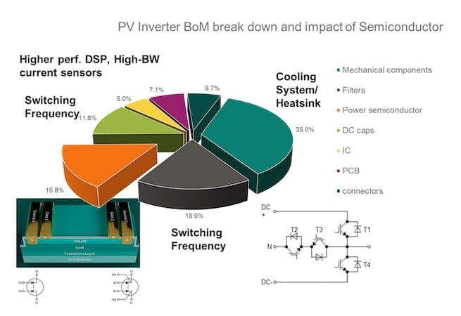
Figure 1. Bill of materials in a typical PV Inverter. Highlighted are how power semiconductors and the auxiliary semiconductors in the system impact the BoM. Further, left bottom new bidirectional GaN switch Technology, and right bottom NPC2 topology. Image used courtesy of Bodo’s Power Systems [PDF]
Among the emerging topologies in solar inverters (as well as ESS and EV charging) are 3-level NPC2 inverters (Figure 1). Compared to the classical Vienna or 2-level bridges, they provide improved power density, more advanced control such as bi-directionality, and better efficiency. Furthermore, such topologies play a crucial role in modern hybrid inverters, which connect PV to the grid, ESS, and power sinks. Providing the right power semiconductors for these topologies can have a considerable impact on both the cost of manufacturing and ownership of the system. In Figure 2, using Infineon Technologies’ CoolSiC Gen2, the efficiency of both the DC-DC converter (battery side) and DC-AC inverter is shown. It can be seen that using a full SiC solution, which is optimized for the application, improves partial load efficiency by more than 1 percent, and even full load efficiency is significantly higher. These improvements, stemming from the choice of topology with the right fit semiconductor, result in considerably reduced cost of ownership and operation due to significant improvements of the power conversion efficiency. Moreover, the Infineon SiC MOSFET allows for two times higher switching frequencies than silicon in high power applications, which, as can be seen in Figure 2 (right image), also has a direct impact on inductor volume and hence the cost of magnetics as well as filters. At 40 kHz switching frequency, the relative inductor size reduction that can be achieved is 38 percent. Looking back at the BOM, this means that the semiconductor’s ability to drive new topologies, at different switching frequencies with the required conduction properties, can directly impact the largest contributors to the BOM, namely system mechanics (weight, cooling, and volume), as well as system passives.

Figure 2. Efficiency improvement through utilization of WBG power semiconductors optimized for PV Inverter such as Infineon CoolSiC™ in NPC2 and the impact of switching frequency on the inductor volume. Image used courtesy of Bodo’s Power Systems [PDF]
The NPC2 topology has a further architecture that can be enhanced with the right device, the back-to-back devices in the Tbranch seen in Figure 1, greatly benefit from a technology that would enable a bi-directional switch. Infineon has been working to deliver the most robust, industrial ready bidirectional GaN based HEMT for power applications. Based on the CoolGaN™ technology platform, this unique switch can further reduce component count and complexity in the topology while simultaneously helping to push the boundaries of system cost ($/W) and efficency.
Electrification
A key pillar of the global de-carbonization strategy is the continuous electrification of mobility and transportation. Generally, there are three scenarios: State Policies Scenario (STEPS), Announced Pledges Scenarios (APS), and Net Zero Emissions (NZE). According to the IEA, depending on the scenario, power demand ranges from 2000 TWh by 2035 (for STEPS) to 3600 TWh (for NZE). This includes the power demand for trucks and buses but excludes trains and aviation. According to the European Auto mobile Manufacturers’ Association within the EU, the sales of electric cars grew at three times the rate of charging point installations from 2017 to 2023. To achieve a successful transition to electromobility and meet the targeted emissions goals, charging infrastructure will be key. Given the vast network needed, the required uptime, availability of power, and the efficient conversion, identifying the right trends is not trivial.
Figure 3 summarizes the evolution of some of the key needs for charging infrastructure. It is evident that power conversion losses in the charging infrastructure significantly impact the difference between the power bought and the power sold. This difference is one of the most important financial metrics, alongside the uptime of the systems. So, how can power semiconductors impact these system FoMs?
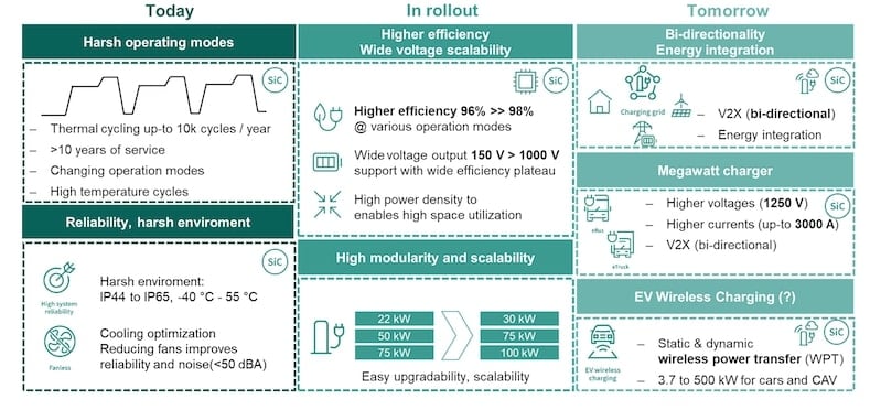
Figure 3. Trends in infrastructure for the electrification of private and commercial transportation. Image used courtesy of Bodo’s Power Systems [PDF]
Charging cycles, particularly in DC-fast chargers, can be very strenuous on the entire system, not only on the car battery but also on the charging station itself. The system typically operates at a specific temperature, sometimes within harsh environments, and needs to ramp up to the maximum currents required to achieve fast charging. Within 10-20 minutes, the user will want to leave, and the charging cycle is finished. This cycle repeats multiple times per day throughout the entire lifetime of the system, resulting in thermal cycling stress on the power semiconductor and its die attach. Infineon has developed a die attach technology family, available for its modules and discrete products, known as .XT joining technology, as seen in Figure 4. This technology not only improves the maximum power capabilities of a package but also enhances its thermal cycling ability.
Achieving higher efficiencies will be key for improving the cost of ownership and maintaining emissions ratings, as charging an electric vehicle should involve as little waste in electric conversion as possible. To accomplish this, power semiconductors must have low conduction and switching losses, and the packaging must be low inductance to reduce parasitic-induced erosion of switching performance. Infineon has developed an array of low inductance discrete and module packaging for their best-in-class wide bandgap and silicon-based power switches. An example of an intrinsically low inductance designed package from discrete QDPAK to modules such as Easy 2B or XHP™2 and their successors and its successor, which despite current ratings of up to 1800 A at 1700 V, come with inductances below 10 nH. Such products are already future proof for mega-watt charging stations required to fuel the electric trucks of the future.
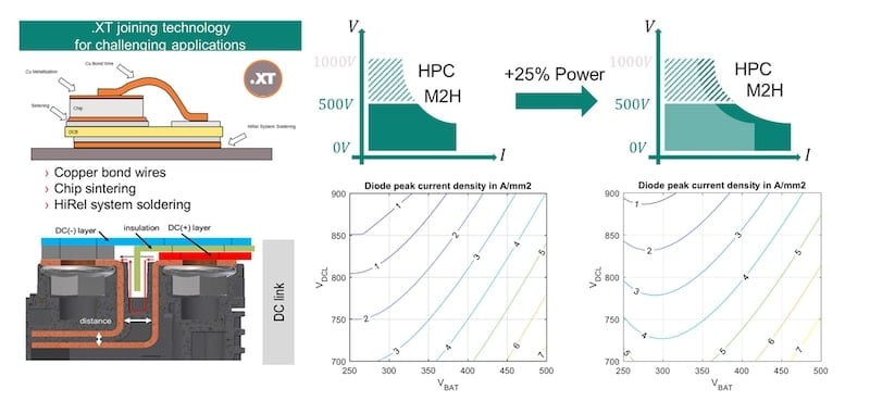
Figure 4. Next generation packaging, die attach and semiconductor technology to meet the needs of modern and future charging infrastructure. Image used courtesy of Bodo’s Power Systems [PDF]
Further trends that are being rolled out or are emerging include wide voltage output range chargers and bi-directional systems. The wide output range of 150V to 1000V is necessary due to the increasing variation among battery voltage architectures in vehicles. The topology of choice for the DC-DC stage of the charger is the dual active bridge (DAB). Since it is a soft-switching topology, it is often overlooked that the body diode plays an integral role in this application. For EV charging stations with a wide output range, the body diode’s ability to carry high current densities becomes increasingly important. As can be seen from the simulation in Figure 4, this characteristic is crucial for efficient and reliable operation. These current densities are close to the limits of bipolar degradation in SiC MOSFETs. Here, Infineon’s decades of research and development have been backed into the technology to provide the best-in-class robustness against bipolar degradation, making it one of the few reliably useable body diodes of SiC MOSFETs on the market.
Solid-State Power Distribution
As the energy generation, distribution, and utilization landscape is transforming, one begs to ask the question: Is our infrastructure smart enough to handle these new sources and sinks with their peculiarities? This brings us to the emerging application of solid-state power distribution and one of its central components, the solidstate circuit breaker. For more than a century, electric power distribution has utilized some form of electromagnetic relays or vacuum tubes to isolate against failures in the distribution network or fault states with connected equipment to the power mains.
However, as our grids become more intelligent and our power sources shift to distributed energy resource systems (DER), it will no longer be feasible to rely on old circuit breaker technology. The future of power distribution will need to support smart billing, even for sub-branches of the distribution network, capture and log data in real time, enable remote load control and diagnostics, support the bidirectional features of loads such as EVs or hybrid inverters, and much more. Such a system will need to support overcurrent protection (OCP), arc fault detection devices (AFDD) / arc fault circuit interrupters (AFCI), and residual current devices (RCD) / ground fault circuit interrupters (GFCI) all in one. It will require highly accurate and user-programmable tripping characteristics to meet the needs of emerging DER grids and provide the fast response time that a protection device must have to achieve selectivity vs. electronic infeed sources, such as PV inverters.. With all the added features, such a system will need to fit into comparable form factors of today’s MCBs. Although much of the intelligence to perform these functions comes from software and microcontrollers, there is a need for a power semiconductor that can not only provide the cost/performance ratio to make such an application commercially viable but also survive the unprecedented stresses that classical electromechanical relays and vacuum tubes have endured for decades.
At PCIM 2025, Infineon will unveil an application-derived power semiconductor technology, based on silicon carbide, that has been designed from the ground up to meet the needs of solid-state power distribution applications. The basic set of requirements that laid the groundwork for defining this new technology is shown in Figure 5.
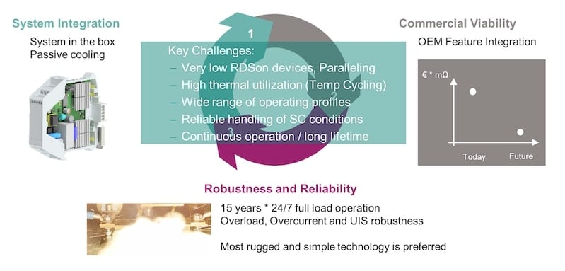
Figure 5. Requirements for a solid-state circuit breaker, derived from the operating and failure conditions that a system will need to survive. Requirements are not limited to technical but also commercial success. Image used courtesy of Bodo’s Power Systems [PDF]
This technology must provide a Ron*A that is much better than the best-in-class Infineon SiC MOSFET, offering unprecedented conduction losses and enabling passive cooling. Additionally, this device must be able to reliably handle short circuit and avalanche failure cases, a feat typically within the RDSON trade-off regime of any SiC MOSFET. The advanced features resulting from an application centric derivation of a product can be found in Figure 6.
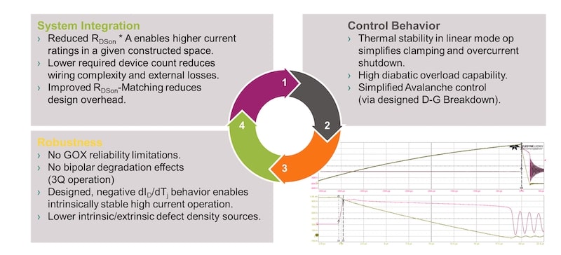
Figure 6. A New technology developed by Infineon to meet the needs of solid-state power distribution shows here how the switch is reliability turning off >10x over current in a system rated for 63 A. Image used courtesy of Bodo’s Power Systems [PDF]
This new device has been specifically designed to excel in its ability to be easily integrated into high power density designs and to be easily paralleled. Furthermore, given the need for a power distribution system to be on 24/7, 365 days a year until a fault happens, the sources of failure in a MOS technology have been eliminated, and robustness has been enhanced to meet the stringent requirements of protection and grid connected systems. Hence, this new technology does not have a gate oxide, bipolar degradation effects have been further improved, and the focus is set on lower intrinsic/extrinsic defects. Beyond the ability to achieve unprecedented power densities and robustness, control behavior has been an essential design parameter. It is expected that the device behaves in a controlled manner under thermal stress, overload conditions, and during failure modes. In figure 6, tests show that this technology can safely turn off a system designed for 63 A at >1 kA in overload.
This groundbreaking technology, along with its platform rollout featuring both 750 V and 1200 V devices, will revolutionize power distribution and propel it into the age of semiconductor-based smart power distribution, redefining the industry’s standards and capabilities.
This article originally appeared in Bodo’s Power Systems [PDF] magazine. Special thanks to the System Architecture and Application Marketing team at SAS, including, Markus Hermwille, Leo Aichriedler, Peter Slama, Tizian Senoner, Torsten Klemmer, Martin Warnke, Gerald Wriessnegger, and Suresh Thangavel for their contributions.