Facebook
 Google
 GitHub
 Linkedin
Practical Solutions Design with GaN Power Transistors
This article discusses the advantages of Gallium Nitride over Silicon Carbide in terms of performance and application.
Analyst firm IHS is projecting continued growth in the power semiconductor market with Wide Bandgap (WBG) devices in the 100-650V range to have the greatest overall gain. Among WBG semiconductors, GaN is fast becoming the leading transistor technology with the many successes companies are realizing with GaN devices.
Its use in power is being proven in designs ranging from power supplies in data center servers and racks, computing and communications systems to renewable energy systems (e.g. solar energy storage systems and inverters), motor drives and pumps, class D audio systems, and electrification of transportation (e.g. EV wireless battery charging systems and automotive onboard chargers). Improvements in other power electronics systems such as high-speed wireless charging and AC adapters in consumer applications are easily achieved.
The largest growth markets for WBG semiconductors including GaN are in automotive and transportation, which is projected to exceed $7.1 Billion USD by 2023, industrial systems (to exceed $10.5 Billion USD), and consumer electronics sector (to exceed $6 Billion USD). Other industries are worth looking at as well. The computing, datacenter, communications, and datacom (5G enablement)/telecom sector will also grow with rising appetites from consumers for greater speed, data, and convenience. This is accelerating the need to upgrade the power supplies in areas such as data centers for greater efficiency, scalability, and flexibility as that market becomes a higher percentage of the overall power demand.
In all, the common theme is the insatiable appetite for greater efficiency in all these applications. The largest percentage of growth in WBG semiconductors, which will have the greatest impact as the need or increasing efficiency, reducing size, weight, and power density and overall systems cost, is most proximate in applications from 20W to 20KW. These applications are moving forward at an ever-increasing pace due to the tremendous benefits to the end user.
GaN Performance Advantages
One of the biggest advantages of GaN is offering better high frequency and high voltage performances that results in developing power device designs that are smaller in size and reduce cost. In the ease of evaluation in new designs, GaN E-HEMTs already use similar techniques to what power electronics designers use today. GaN Systems e-mode devices use comparable techniques for maximizing efficiency of their designs by providing similar gate drive signals and PCB layout techniques can be used so the learning curve is very short.
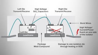
In our case, it’s very easy to take advantage of the higher frequency operation and low parasitic inductance, which has already been taken care of by our GaNPX® Packaging – making it easy by supplying SPICE models, thermal models, schematic symbols and PCB footprints for incorporation into PCB development and layout software packages. In comparison to the industry’s legacy packaging approaches such as TO-247 and PQFN, GaNPX is designed to lower the possibility of failure and maintain the power efficiency benefit that GaN technology uniquely provides through the production process.

Figure 1: Designed to lower the possibility of failure and maintain the power efficiency benefit that GaN technology provides
As the gate drive of GaN Systems devices are similar to existing silicon MOSFETs, many of the existing isolated and non-isolated gate drivers can be used. In fact, with lower gate capacitance they are often easier to drive. This, combined with the existing nature of GaN makes them as close to as MOSFETs as possible but much faster thus getting closer to the ideal switch needed in power electronics designs.
Due to the benefits of GaN EHEMTs in power in conversion, many existing and new IC suppliers are developing GaN drivers to further optimize these benefits. If higher currents are needed, GaN Systems devices are easily paralleled and the lower gate charge capacitance makes them easy to drive while increasing speed and circuit efficiency.
GaN comparison to Silicon Carbide (SiC) – Performance and Application
Any non-ideal semiconductor switches will have loss contributions. When compared to traditional silicon switches, GaN devices exhibit the following properties.
- Lower “Conduction loss” that is due to the DC resistance in the device current loop.
- Lower “Switching loss” that occurs during the transition between “On” and “Off” states.
GaN devices can cut power conversion losses from the state of what’s possible today with silicon switches by 50-90 percent.
We can see that GaN has clear advantages when compared to silicon. However, what about comparisons to SiC? Power devices today are increasingly based on SiC and GaN as both have material properties superior to traditional silicon.
However, there are some comparisons to note between GaN E-HEMTs and SiC MOSFETs in performance and in certain applications. In many applications, GaN E-HEMTs exhibit much higher efficiencies than ones that use SiC MOSFETs and exceeds the performance in terms of switching speed, parasitic capacitance, switching loss, and thermal characteristics. Compared with SiC counterparts, GaN E-HEMTs facilitate the construction of significantly more compact and efficient power converter designs.
With the same layout design, it has been shown and demonstrated that GaN devices exhibit four times faster turn on and two times faster turn off time in actual operating converters. This means, three times less switching losses and 40-60C degrees lower temperature operation while giving one percent greater efficiency in a sync buck converter. These are critical advancements towards the ideal switch and we are closer than ever before to achieving this theoretical limit.

Figure 2: Four times faster turn ON and two times faster turn OFF time in actual operating converters
What else can be done other than simply improving existing topologies?
GaN offers opportunity for topologies
GaN offers the opportunity to create new topologies and enhance existing ones, which in many cases allow the reduction of component counts while increasing reliability at the same time. The bridgeless Totem pole topology is now easily enabled with GaN Systems devices. Since GaN devices have no parasitic BJT or body diode and offer zero reverse recovery charge, designers can implement topologies that take advantage of these characteristics. One of the efficiency limitations for AC offline applications has been the input bridge rectifier. By implementing the bridgeless totem pole architecture, the input bridge rectifier can be eliminated and stages can be combined.
In other words, if rectification from the mains can be combined with the PFC function then we can achieve several benefits at once to increase the overall power converter efficiency by eliminating the forward voltage drop of the bridge rectifier. No body diode results in zero reverse recovery charge however, it is reverse conduction capable without the need for an anti-parallel diode. External parts count is reduced as well.
GaN reduces losses, increases efficiency, and reduces size
GaN reduces losses, increases efficiency, and reduces size as less heat sinking is required, and the size of magnetics components decrease. In DC-DC designs especially in the ZVS (Zero Volt Switched) LLC converter, GaN technology contributes reduced output capacitance, COSS, which makes the converter not only easier to achieve ZVS, but also reduces the transformer losses and RMS currents. This translates to smaller magnetics resulting in higher efficiency typically by 50-90 percent, smaller size (quarter of the original size in many cases), and higher power density.
Moreover, the weight is also reduced to a quarter of the non-GaN implementation weight. GaNPX packaging technology also creates flexible and innovative thermal solutions. For example, GaN Systems offers IMS modular evaluation platforms up to and greater than 5KW, which incorporate commonly used topologies such as half bridge and full bridge converters for ease of trial in applications.

Figure 3: GaN reduces size as less heat sinking is required
A Ready Ecosystem of Support Components
GaN covers almost any design need from 100Vat 90A to 650V at 60A today. It’s also never been easier to use GaN with a robust ecosystem of support component – gate drivers, controllers, magnetics and module partnerships in place. Additionally, GaN Systems has invested in developing this network with industry leaders, which enables new topology implementations that further increase efficiency of new designs while reducing component count.
Conclusion
In many applications, the superior thermal performance and cost effective GaNPX packaging makes implementation in any design easy while making it possible to reduce system cost, increase reliability by lowering heat dissipation, lower shipping costs via smaller size and weight, and reduce maintenance and system operating costs.
All of these benefits combined with an ecosystem of support components result in a lower bill of materials cost, lower shipping and installation costs, lower operating costs, and lower maintenance and repair costs, resulting in lower total cost of ownership. While we have just scratched the surface here we invite you to view the entire presentation and explore what’s possible in creating designs with a competitive edge and adding more value to your end customers. View the presentation with this link.
About the Author
Peter Di Maso holds an MBA at Southern New Hampshire University and a Bachelor's Degree in Electrical, Electronics and Communications Engineering at Concordia University. He specializes in semiconductors, power management and integrated circuits. He currently works as the Director for Product Line Management at GaN Systems Inc.
This article originally appeared in the Bodo’s Power Systems magazine.