Facebook
 Google
 GitHub
 Linkedin
Power Module Solutions for a 1500V PV Inverter
The elevated operation voltage of 1500 V has become the new photovoltaic standard and requires new and smart power module solutions for a simplified topology and lower system cost.
Photovoltaic systems have seen enormous growth during the last decade. The economy of scale and innovations in the area of system technology, which are leading to a reduction of the levalized cost of energy (LoCE), are among the main drivers behind this development [1]. Moreover, a shift in DC system voltage from 1000 V to 1500 V can be observed in utility-scale systems [2]. The implementation of this increased operation voltage started from the low power class with its string- and residential inverters in the past, now followed by the megawatt (MW) classes of the solar central inverter. Nowadays the operation voltage of 1500 V is the established standard for all the different power classes in the solar application area.
The high operating voltage of 1500V results in the requirement of a low, cosmic radiation-induced failure rate [3], with high system efficiency for the power devices at the same time. Because of these contradictory requirements, NPC1 or A-NPC multilevel topologies are the preferred solutions today [4]. Multilevel topologies such as NPC1 constructed using single power modules face various challenges. For example, the loop inductance (LS) is typically very high and could be in the region of Ls>100nH. High voltage overshoots during IGBT turn-off due to the high loop inductance require safety features like overvoltage clamping with a sophisticated gate drive unit (GDU) [4].
2300V: A New IGBT Voltage Class for 1500V PV Central Inverter
Because of all these challenges in this field of applications, Infineon Technologies developed a new voltage class [5] for power modules without all these restrictions. Consequently, the new power devices are determined by the cosmic radiation robustness requirements. The clear focus is set on the MW-range of solar central inverters with VDC=1500 V and results in the new 2300 V Si-IGBT and 2300 V Si-Diode voltage class. To reach the highest performance, the most recent technology with the 7th generation of the TRENCHSTOP™ IGBT and Emitter Controlled Diode is used as the basis for this new power device.
The maximum continuous operating temperature for the semiconductors is set to Tvj_max=150°C combined with the extended usable overload temperature. This enables using the operating temperature close to the maximum permissible junction temperature of Tvj_max=150°C of the modules. The extended overload temperature (TvjOL) allows the device to be used up to TvjOL=175°C for short periods of time, to cope with short-term overload operation during grid fault events.
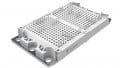
Implementing the new chipset in the PrimePACK™ 3+ housing, a new high current power module in half-bridge (FF) configuration with a nominal current rating of 1800 A is feasible and results in the new module type FF1800R23IE7 with full current rated IGBTs and full current rated diodes. This new power semiconductor solution allows a flexible and simplified inverter design for solar central applications in a standard standalone 2 level (2L) topology. It is also an excellent choice as the main part in an efficient 3 level NPC2 topology (3LNPC2).
For the standard 2L topology, the full system operating voltage in a solar central inverter between DC(+) and DC(-) is given with VDC=1500 V. Figure 1 shows the IGBT turn-off event of the FF1800R23IE7 in such a 2L setup with VDC=1500 V, room temperature and with a collector current of IC=1800 A.

Figure 1: IGBT turn-off FF1800R23IE7 2L; VDC=1500 V, IC=1800 A, Tvj=25°C
The resulting overvoltage peak is only ΔVce=312 V and results in VCEpeak=1812 V under these conditions which are far below the 2300 V. This new 2300 V PrimePACK 3+ power module can be combined with a further new 1200 V PrimePACK 3+ module in a common collector configuration to achieve a high current solution in a 3L-NPC2 topology.
Power Modules for 1500V 3L-NPC2 Solar Central Topology
This 1200 V common collector (CC) PrimePACK 3+ module is based on the latest TRENCHSTOP IGBT7 technology from Infineon Technologies [6] with the correlating temperature features. The CC topology is designed for the bidirectional switch in the NPC path of a 3 level NPC2 topology. This device needs to handle high currents during the regular operation as well as overload conditions during grid fault events.
With respect to such regular and irregular operation conditions, as well as to provide the opportunity for achieving maximum power, the new device FF2400RB12IE7 provides a nominal current rating of ICnom=2400 A. The proposed NPC2 solution can, therefore, be assembled in a two-module (1:1) configuration and upgraded in power in a three-module (2:1) configuration. The basic schematics for both variants are depicted in Figure 2.


Figure 2: a) NPC2 topology with two PrimePACK™ 3+ power modules 1:1 (1 half–bridge + 1 common collector); b) with three PrimePACK™ 3+ power modules 2:1 (2 half–bridges + 1 common collector
Minimizing the loop inductance at the system level is a key lever for optimizing the overall system performance. A bidirectional switch implemented within a single package results in a lower parasitic inductance in the three-level system compared to a solutions based on series-connected, single-switch modules. With the four separate module-internal bus bars of the PrimePACK 3+ package, a low parasitic inductance is achieved with high current carrying capability at the same time. The staggered power terminal design of this concept offers the possibility of a reduced overall system inductance. As each bus bar pair forms a strip line conductor, the stray inductance is reduced. In Figure 3, the module arrangement and a possible DC-bus structure for a three-module (2:1) phase is shown. In the center of picture 3 A, the power terminal layout of the CC module is illustrated.

Figure 3: a) Exemplary module arrangement of two FF modules and one CC module with staggered power terminals; b-d) DC-bus bar layers and structure DC(+)/AC à NPC à DC(-)
For the 3L-NPC2 1:1 module arrangement, the loop inductance will increase moderately compared to the 2:1 solution. A loop inductance of such a 1:1 system of approximately Ls=35 nH is feasible. The resulting peak voltage for the 2300 V FF device and for the 1200 V CC device in such a 1500 V set is of interest. For a worst-case peak voltage investigation, the full system operating voltage from DC(+) to DC(-) with VDC_System=1500 V is applied in an exemplary lab measurement. The effective voltage for these measurements from DC(+) to neutral (NPC) and from neutral (NPC) to DC(-) results in VDC=750 V because of VDC=VDC_System/2. In Figure 4, the measured peak voltages VCEpeak are shown for both devices at 750 V, room temperature, and rated device currents based on the most recent sample status for both devices.

Figure 4: a) IGBT turn-off FF1800R23IE7; VDC=750 V, IC=1800A, Tvj=25°C; b) IGBT turn-off FF2400RB12IP7; VDC=750 V, IC=2400 A, Tvj=25°C
For the FF1800R23IE7 the peak voltage is measured with only VCEpeak=1080 V and for the 1200 V bidirectional switch, the peak voltage is only at VCEpeak=1064 V under these conditions. All peak voltages are well below the rated maximum of the individual devices. All measurements were conducted without the usage of active clamping measures. The results offer the opportunity to operate these power modules without overvoltage limitation during regular operating conditions. The obvious advantage is a reduced amount of components and a further step forward for simplified inverter design.
Figure 5 summarizes the simulation results considering a variety of potential solutions regarding high-power central inverters. For the simulation, not the worst-case maximum operation voltage but more application relevant reduced bus voltage of VDC=1200 V for the PV system is assumed. For the 2-level configuration with two modules per leg (2L-2M) the power of 800 kW per inverter looks feasible, whereas the three-modules configuration (2L-3M) offers the possibility to reach 1200 kW. For both configurations, a discontinued pulse width modulation (DPWM) was considered.

Figure 5: Simulated output power of a 2 level, a 3 level NPC1 and the 3 level NPC2 set up with the new solution
In comparison to the standard two-level topology, the reduced losses and the significantly increased efficiency of the three-level topology results in the same or higher output power.
Comparing the different three-level solutions, the new three-level NPC2 configurations looks the most promising. The same output power is reached with a lower number of modules, two modules (3L-2M) instead of three modules Alternatively, the same amount of modules (3L-3M),achieves 1600 kW which is approximately 33 percent higher output power on the same total module footprint.
Not only the high-power PV central inverter had to follow innovations to support further steps in the field of PV system technology, but also the string inverter.
Power Modules for 1500V 3L A-NPC String Inverters
A cost-efficient way for a special adaptation of the A-NPC topology to optimally combine Infineon´s CoolSiC™ 1200-V MOSFET with TRENCHSTOP IGBT technology is proposed. An output power of 75 kW at a switching frequency of 35 kHz is possible with the presented EasyPACK™ 2B power module. By paralleling, the output power is increased accordingly. Moreover, an almost circular P-Q diagram is achieved which supports emerging applications such as energy storage systems.
A shift in DC system voltage from 1000 V to 1500 V can be observed in utility-scale systems [2]. The main motivation is the reduction of cable and installation costs as well as the improvement of system power density due to high DC and AC voltage levels. Moreover, decentralized high-power string inverters in the range of 75 kW to 150 kW per unit are emerging in utility-scale systems, as they allow a more flexible design and lower maintenance cost. In addition, energy-storage systems that use DC-voltages up to 1500 V are also becoming more prominent.
Infineon´s CoolSiC MOSFETs perfectly fit into solar applications. Especially with respect to their fast-switching capability and cosmic ray robustness. Even though SiC devices are pricey and the required gate-driver concepts are more sophisticated with respect to, e.g., active-miller clamping for suppressing parasitic turn-on, significant improvements are achieved in terms of losses. Thus, for fast-switching devices, CoolSiC MOSFET is a remarkable alternative solution if combined with cost-optimized silicon devices. By this approach, the switching frequency can be increased, total losses are lowered, and relevant critical components such as filters or heatsinks can be minimized which finally leads to optimized and lowest system cost.
An important feature of high-power string inverters is the ease of installation. It is beneficial if only two workers are able to carry and install the system. This means, that size and weight are of special importance, and thus switching frequency should be as high as possible in order to minimize the output filter. Depending on the topology, not necessarily every switch has to be based on SiC. To achieve an optimum cost-performance-ratio, the use of the right technology with the respective benefits has to be considered. From a system point of view, SiC MOSFET/Si hybrid solutions are the best choice with respect to performance and cost.
To implement 1500 V high-power inverters, the NPC1 topology with 1200 V IGBTs is a common approach today [2]. The Active Neutral Point Clamped (A-NPC) topology with active switches in the neutral path offers an additional degree of freedom.
Figure 6 a) shows a phase leg of the proposed implementation, whereby T1 to T4 are composed of Si-based IGBTs with corresponding Si-freewheeling diodes (FWD). Transistors T5 and T6 consist of CoolSiC MOSFETs with internal body diodes. In contrast to other SiC MOSFETs in the market, no external SiC FWDs are needed. This allows combining all parts in one EasyPACK 2B module, which supports compact designs and high power density. Using the modulation scheme presented in [7], Fgure 6 b), the IGBTs only reverse the polarity of the fundamental output voltage and are switched with grid frequency (50/60 Hz). Hence, the IGBTs can be optimized for the lowest conduction losses.
In this way, switching losses only occur in fast and highly efficient SiC components. Thus, the amount of SiC devices is reduced to a minimum, achieving an optimal cost-performance ratio.

Figure 6: a) ANPC topology in an EasyPACK restricted Copyright © Infineon Technologies AG 2020. All rights reserved. TM 2B power module Infineon Proprietary 6 with CoolSiCTM MOSFET; b) Modulation scheme: T6 operated complementarity to T5.
The junction temperatures of the CoolSiC MOSFET, the Si IGBT and the Si diode, under typical application conditions, are plotted exemplarily in Figure 7. The temperature of the CoolSiC MOSFET (T5) is typically the highest but still well below 150°C. It is practically independent of the power factor. When reaching almost cos(φ)=-1, the temperature of the FWD D1 is similar to that of T5.

Figure 7: Simulated junction temperatures as a function of power factor (Igrid=72 A, VDC=1200 V, Vout=600 VAC, fsw=35 kHz, TA=45°C, TH=90°C)
A significant advantage of the proposed modulation scheme, in combination with the A-NPC topology, is the ability to work in an almost circular P-Q diagram without a current derating on the SiC devices. The diagram is given in Figure 8.

Figure 8: Simulated P-Q diagram (VDC=1200 V, Vout=600 VAC, fsw=35 kHz, TA=45°C, TH=90°C)
This allows using this solution in reactive power mode for regions with unstable grid conditions. This is becoming a more important requirement in utility PV applications. Moreover, the same hardware platform could be used to serve both solar and energy storage applications.
Summary
Newly developed PrimePACK 3+ IGBT power modules rated at 2300 V and combined with newly developed 1200 V modules in common collector configuration support NPC2 solutions. Based on the low inductive DC bus design, the resulting collector-emitter peak voltage is far below the blocking voltage limit of the device. These excellent results offer the opportunity to operate these power modules without overvoltage limitation during regular operation conditions and offer a flexible design possibility at the same time. The two-module configuration reaches a comparable output power level as the 1200 V based NPC1 with three modules. The three-module NPC2 delivers 33 percent higher output power with the same number of modules as needed for the NPC1 topology. All measurements and simulations were done with the current prototypes. Further samples of these prototypes will be available soon
For 1500 V grid-tied converters in the range of 75 to 150 kW, highly compact and efficient power electronics solutions are required. A highly efficient and low-inductive EasyPACK 2B module with a fully integrated A-NPC topology offers such high power densities. The beneficial combination of Infineon´s CoolSiC MOSFET and Si TRENCHSTOP technology in one EasyPACK 2B module combines the best of two worlds. A significant advantage results from the chosen modulation scheme in combination with the ANPC topology. It allows operating the inverter in an almost circular P-Q diagram without a derating on the SiC devices. Based on this characteristic, very flexible usage of the power module for applications requiring a reactive power mode becomes an option. The benefit is to enhance grid stability and to use the same hardware in energy storage systems [8].
About the Authors
Wilhelm Rusche works as the Technical Marketing - High Power Innovation at Infineon since October 2014 where he is responsible for the definition and specification of new products in power electronics. He is a Graduate Engineer in Electrical Engineering at the Comprehensive University Paderborn Dept. FH Meschede.
Jens De Bock holds a Diplom-Ingenieur in Electrical Engineering and Electronics at the University of Applied Sciences South Westphalia. He is skilled in the field of power electronics, product management, and in semiconductors. He currently works as the Technical Marketing Manager at Infineon Technologies located in Germany.
References
- S. Araujo et al. „Exploiting the Benefits of SiC by Using 1700 V Switches in Single-Stage Inverter Topologies Applied to Photovoltaic Systems”, PCIM Europe, 2011
- M. Slawinski et al. “Evaluation of a NPC1 phase leg built from three standard IGBT modules for 1500 VDC photovoltaic central inverters up to 800 kVA”, ECCE Europe 2016
- Soelkner, W. Kaindl, H. Schulze, G. Wachut, “Reliability of power electronic devices against cosmic radiation-induced failure”, Microelectronics Reliability, 2004.
- X. Hao, K. Ma, J. Zhao, X. Sun: “Design of NPC1 power stack beyond megawatt for 1500V solar inverter application”, Proc. IFEEC 2017-ECCE Asia 2017
- F. Umbach, P. Brandt, S. Mansueto, W. Rusche, A. Korzenietz et al.: “2.3 kV – A new voltage class for Si IGBT and Si FWD”, Proc. PCIM Europe, 2020
- J. Esch, S. Mansueto, W. Rusche, K. Yilmaz, S. Thangavel, “PrimePACK™ with 2300 V and 1200 V TRENCHSTOP™ IGBT7 enabling 1500 V-DC NPC2 in MW solar central inverter”, PCIM 2020, Nuremberg, Germany
- D. Floricau et al. “The efficiency of three-level active NPC converter for different PWM strategies,” EPE, 2009 [8] B. Sahan et al. “Combining the benefits of SiC T-MOSFET and Si IGBT in a novel ANPC power module for highly compact 1500-V grid-tied inverters”, PCIM Europe, 2019
This article originally appeared in Bodo's Power Systems Magazine.