Facebook
 Google
 GitHub
 Linkedin
Moving from IGBT to SiC: PFC Efficiency
The continuing worldwide efforts to reduce carbon emissions have driven the growth in interest in electric vehicles (EV). As a result, the demand for a refuelling infrastructure to recharge them is also increasing. Over the course of a few years, millions of charging points capable of delivering between 3.6 kW and 22 kW will be installed, with fast-charging solutions peaking at 150 kW.
Not only must this massive increase in load be supplied and managed, but the charging solutions installed must also play their part by making use of the latest technology to attain the highest possible efficiencies and unity power factor (PF). Power Factor Correction (PFC) stages have been standard in electrical equipment since the European Union established limits on harmonic currents. Power supplies with an input power of 75 W or greater must conform with EN61000-3-2.
Furthermore, market demands are placing pressure on the volume of design and heat dissipation, with a general trend to move towards passive cooling where possible. This puts pressure on designers to find more efficient approaches to their power converter designs. Until recently, PFCs have been the domain of silicon IGBTs, leveraging their high VCES, current handling capability, and robustness. However, the introduction of wide-bandgap power devices is changing the way PFCs are implemented.
Silicon carbide MOSFETs for PFCs
Wide-bandgap technologies, such as silicon carbide (SiC), open up a range of new possibilities for the designers of power converters. Compared to existing IGBT devices, SiC offers significant reductions in turn-on and turn-off losses, as well as improvements in conduction and diode losses. Careful analysis of their switching characteristics shows that SiC MOSFETs fully turn on almost immediately, whereas IGBTs display a significant slope by comparison. This results in a substantial drop in Eon energy losses.
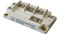
Operating a fast-switching IGBT and Toshiba TW070J120B SiC MOSFET under the same laboratory conditions showed that switching losses in the SiC MOSFET lay at 0.6 mJ. This was around a quarter of the 2.5 mJ measured for the IGBT. In each case, testing was undertaken at 800 V, drain/source current of 10 A, ambient temperature of 150 °C, and optimal gate-emitter threshold voltages (Figure 1).

Figure 1. Compared to latest-generation IGBTs, the TW070J120B SiC MOSFET shows considerably faster switching speeds that deliver higher efficiencies in power converters. Image used courtesy of Bodo's Power Systems magazine.
Simulated in a 3-phase, 400 V PFC, the SiC MOSFET shows application benefits over the IGBT. Factoring in all switching losses, on resistance related conduction losses, and forward voltage loss of the internal diode, a SiC MOSFET-based design saves around 66% in losses over a comparable IGBT-based design (Figure 2). This efficiency improvement provides designers room to reduce the volume of their PFC designs if designing to deliver the same power, or increase power in a design of the same volume.

Figure 2. Implemented in a 3-phase PFC, the SiC MOSFET shows a 66% reduction in power loss compared to an IGBT-based design. Image used courtesy of Bodo's Power Systems magazine.
The integrated diode of the TW070J120B provides an excellent forward voltage (VDSF) of just -1.35 V (typical) that is also very robust to current surges, handing current pulses of up to 72 A (TC = 25 °C). The -10 V to 25 V gate-source (VGSS) is wider than competing products, facilitating easier design, while the high gate threshold (Vth) of 4.2 to 5.8 V protects against unwanted switching due to gate voltage fluctuations and noise.
Accelerating SiC-based PFC design
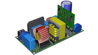
While the move from silicon IGBT to SiC MOSFET in power converters is relatively straightforward compared to other Wide Band Gap (WBG) technologies, access to reference designs is universally recognized as being the fastest way of mastering new technologies. The Toshiba 3-phase, 400 V AC input PFC reference design has been specifically designed with applications such as EV charging in mind (Figure 3).

Figure 3. The TW070J120B SiC MOSFETs are coupled with the TLP5241A gate driver in Toshiba’s 3-phase, 400 V PFC reference design. Image used courtesy of Bodo's Power Systems magazine.

Figure 4. The Toshiba 3-phase, 400 V PFC reference design is ideal for use with bidirectional DC-DC converters in battery charging applications. Image used courtesy of Bodo's Power Systems magazine.
Generating a 750 V DC link output, it achieves a conversion efficiency of 97% and a power factor of 0.99 or better. It uses a bridgeless 3-phase totem pole design, switching each phase directly from a 50 or 60 Hz line of between 312 V AC and 528 V AC. The design is suited for use with bidirectional DC-DC converters to implement EV battery chargers for which a further reference design is currently being developed (Figure 4).
The reference design couples the 1200 V TW070J120B SiC MOSFETs with the TLP5214A gate drivers to attain optimal performance. This allows switching frequencies of 50 kHz to be used, higher than those allowed by IGBTs, leading to a reduction in both the size of the inductors and power converter. The higher switching frequency can lead to challenges in fulfilling EMI requirements. Gate drive circuit switching speed can, however, be easily tuned, albeit at the expense of overall efficiency.
Critical to optimal control of SiC MOSFETs is the application of the correct gate signal, and it is essential to adhere to the application of gate voltages as defined in the datasheet. The reference design ensures that this always lies between the specified -10 V and 25 V. The turn-on voltage is set to lie between 18 V and 20 V, while the turn-off voltage is configured for between 0 V and -5 V.
At turn-on, the gate requires 70 nC, so the gate driver must be capable of providing this energy at the switching frequency selected. The TLP5214A used comfortably sinks and sources up to 4 A, which is enough to drive and discharge the gate of the TW070J120B. Additionally, it is equipped with overcurrent and undervoltage lock-out protection for robust handling of system abnormalities.
Summary
The rapid adoption of EVs is bringing the challenges of keeping them fuelled into sharp focus. With the high-power levels involved, every percentage point of inefficiency results in hundreds of Watts of wasted energy. While IGBTs have traditionally been relied upon for the bulk of active PFC designs, next-generation designs demand higher performance that pushes efficiency to the limit of what is possible. SiC, a robust and high-voltage-capable WBG technology, is displacing IGBTs in such applications. Thanks to carefully designed reference designs, such as Toshiba’s 3-phase, 400 V PFC, engineers are able to not only quickly evaluate such designs but also acquaint themselves with SiC MOSFET technology, allowing them to develop stable and reliable power converters rapidly.
This article originally appeared in Bodo’s Power Systems magazine.