 Facebook
 Google
 GitHub
 Linkedin
Measuring Conduction Voltage of Semiconductors in Operation for Real Time Temperature Evaluation
Junction temperature is directly related to system reliability. With TO packaged transistors, it was possible to add a thermocouple to the case and get a good idea of the junction temperature this doesn’t work for most SMD parts
Directly measuring the junction of SMD components is almost impossible, for the following reasons. There is no space for placing a thermocouple which can also influence the measurement. Top cooled cases allow us to measure the heatsink temperature, but poorly defined thermal resistance between transistor and heatsink, makes impossible to reliably calculate the junction temperature. In product development, worst case junction temperature is often estimated based on data sheet values of Rth. Production end tests measure many electrical parameters, but I have never seen the junction temperature being checked. Although this is critical for reliability. I remember 2 cases of early device failure, due to bad mounting of TO247, transistors. The leads were stiffer than the heatsink clips, so the cooling tab did not lie flat on the heatsink.
Often the weak link in the cooling system is the thermal interface material (TIM) between the transistor and the heatsink. The power density is highest and the thermal resistance poorly defined. To keep thermal resistance low, a thin thermal interface material with high conductivity and low elasticity is used. The package dimensions of modern WBG transistors can have tolerances of over 300µm, and the TIM used is often thinner than the tolerances, to keep thermal resistance low. Figure 1 shows an exaggerated worst case, with the middle transistor higher than the outer devices.

Figure 1. Poorly cooled transistors influence reliability.
The outer devices Q1 and Q3 will be badly cooled and run hotter than designed. Other factors such as solder thickness, foreign particles, pcb copper planarity etc only add to the tolerances.
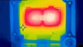
In design qualification, thermocouples or thermal imaging are often used. A thermal camera looks through the package at the junction; the hot spot could be detected (figure 2); from here on we need a “magic factor” to arrive at an estimated junction temperature.

Figure 2. MASTERGAN1 hotspot measured, unknown junction temperature
This gives a number with an unknown accuracy, but even this cannot be used when a top cooled package is used. Here the heatsink is mounted over the transistor, there is usually no thermal connection to the backside of the pcb and the transistor is so small there is no possibility of reliably attaching the thermocouple to the device pad.
Real-Time Junction Temperature Evaluation
Modern HEMTs and FETs, have a clear dependency between Rdson and temperature. The conduction voltage of Schottky and SiC diodes can also be temperature dependent. Despite its dependence on current and gate voltage, the conduction voltage still gives very good indication of the junction temperature. The various component technologies have different characteristics and for SiC and GaN the device design, saturation currents and dynamic Rdson also play a role, so the exact operating conditions are needed for a reliable estimation of the junction temperature. This is particularly important during design qualification, where a reliable measurement is the basis for the approval and field reliability prediction. In production testing and quality assurance, where the build quality is being tested, a comparison of the semiconductor conduction voltage under the same test conditions between production units under the same operating conductions gives a good indication if the thermal management is working as designed. Hot parts generally have a higher conduction voltage.
Compared to the older TO-220 transistors, the modern transistor packages have a small thin contact area with little copper and a very low thermal mass. With little to heat up the temperatures rise fast. When the heat is not being properly carried away by the cooling system, 2W losses heat up an SMD transistor junction at about 36°C/s. This is fast enough and large enough to be easily seen in a production end test during the normal full load power testing.

Figure 3. MasterGan hot Rdson measurement in 500nS
Testing in practice is very simple; a Springburo clipper or similar can be used and simply connected over the transistor. An optional quality 10:1 differential probe can reduce potential issues with circulating currents. The clipper cuts out the high switching voltage over the DUT, so the conduction voltage can be seen in detail. We use a scale about 200mV/div. To calculate resistance a current signal also needed. Most modern DSO can then perform a math function as shown in Figure 3. The math channel shows the Rdson at about 211mΩ, this is 150% of the measured cold value of 140mΩ. For the datasheets, this means the junction is about 77°C, significantly hotter than 49°C shown in the thermal image in Figure 2.
In Figure 3, the displayed Rdson takes about 500ns to stabilize, this is because a lazy setup was used with long wires to the clipper; as would be the case in a production environment. If faster measurements are needed then the clipper must be connected directly at the component body, to minimize the effects of lead and wiring inductance. Figure 4. shows achievable performance. The settling time is reduced from 500ns to 100ns. The time base is 80ns/div; the MOSFET drains on Ch2@200V; the MOSFET is turned off for about 200ns and then turned on switching 1000V in about 15ns.

Figure 4. Conduction voltage measurement in 100nS after switching 1000V
The clipper output is shown on Ch1@ 100mV, Ch4 is the switch current, with ringing. The clipper output has recovered and is showing the MOSFET has a conduction voltage of about 400mV, slightly lower than before it turned off, 100ns after the switching event. This is because the inductor current has fallen during the off-time. The Rds calculated from the current and clipper voltage; is the same before and after the switching event. This confirms that a fast and accurate measurement within a few 100ns of the conduction voltage is possible, even with an off state of 1000V and a conduction voltage of 400mV. This is useful for evaluating components and ensuring they are being turned on and off properly.
Accurate Measurements Need Care
Measuring the conduction voltage in the application is looking at a few hundred millivolts in hundreds of volts, and then needing an accuracy of a few percent. In the example shown in Figure 4, a 20mV error would give a 5% error in the calculated resistance. 20mV in 1000V is .002% error. This is way outside the possibilities of scope probes. Typical probes specify a DC accuracy of about 2%, (AC accuracy is not specified), well outside the accuracy needed for reliable conduction measurements. (We tried lots of different solutions but needed something easy to use, that we could trust without careful calibration etc).
For junction temperature evaluation, when dynamic resistance or switching characteristics is not the focus, the conduction voltage can be measured in the middle of the switching cycle. This means that very short connections are not necessary. As timing is not important for comparative measurements, common-mode filters can be added to reduce ground ringing. The CLP1500V15 is a passive probe with no offset and with a voltage transfer under the clipping voltage close to 100%. It is not isolated and has a common ground connection with a scope. This works well if the DUT is supplied from an isolated power supply, but even then there is a risk of common ground currents affecting the measurement accuracy. A 100MHz differential probe can be used to block these currents as shown in Figure 5. If large common-mode voltages are present, the differential probe can add significant errors. Alternatively, an optically isolated probe or analogue isolator can be used on the clipper output. A floating isolated scope is another possibility, note we have seen that some scopes don’t like the common-mode switching and behave “strangely."

Figure 5. Lazy measurement setup with long leads, Rds measurement valid after 1µS
Figure 5 shows a lazy test setup, on a flyback power supply. The clipper is connected to the transistor with about 20cm leads. The MOSFET is switching about 900V. When the MOSFET is turned on, the clipper output falls to zero and rises to 3V. The Rds, calculated from the current and voltage is 1.7Ω; close to the typical datasheet value of 1.8 Ω; confirming that even with long leads to the clipper, (such as a production test probe or test point,) good measurement accuracy can be achieved. The settling times are just longer. In the above example 1µS is needed before settling, this is a typical value.
New Possibilities
Being able to “look at the junction” conduction voltage, with the clipper gives new test possibilities for design and production screening. Monitoring transient effects, such as overload or start-up. Recording mains frequency temperature variation in PFC and inverters. Observing junction temperature stress under power boost in new generation SiC and GaN EV inverters, is now a real possibility. The need for Xray control for solder voids under SMD power components could be reduced by confirming conduction voltage and junction temperature in production end tests; or during extra QA testing. Looking for a needle in a haystack can be difficult, but with the correct tools, X-ray or magnetic sensors etc it is easy. Checking semiconductor conduction voltage in operation was once difficult and can now be done fast and efficiently with the clipper.


What is a “Springboro clipper?”
Typo in article “Springboro” should be “Springburo.”
http://springburo.weebly.com/