Facebook
 Google
 GitHub
 Linkedin
Layout Considerations for GaN Transistor Circuits
This article is the first in a series of articles discussing three topics that can help power systems designers achieve the most out of their GaN-based designs at the lowest cost.
Gallium nitride (GaN) transistors have been in mass production for over 10 years. In their first few years of availability, the fast switching speed of the new devices – up to 10 times faster than the venerable Si MOSFET – was the main reason for designers to use GaN FETs.
Introduction
As the pricing of GaN devices normalized with the MOSFET, coupled with the expansion of a broad range of devices with different voltage ratings and power handling capabilities, much wider acceptance was realized in mainstream applications such as DC-DC converters for computers, motor drives for robots, and e-mobility bikes and scooters. The experience gained from the early adopters has led the way for later entrants into the GaN world get into production faster.
This article is the first in a series of articles discussing three topics that can help power systems designers achieve the most out of their GaN-based designs at the lowest cost. The three topics are: (1) layout considerations; (2) thermal design for maximum power handling; and, (3) EMI reduction techniques for lowest cost.
Parasitic Inductance Due to the High Switching Speed of GaN
The use of GaN at higher frequencies than the aging power MOSFET is capable has put a spotlight on the degrading effects of parasitic inductance in a power conversion circuit [1]. This inductance hinders the extraction of the full benefit of GaN’s extra-fast switching capabilities with reduced EMI generation. For a half-bridge configuration, which is used in about 80% of power converters, the two main sources of parasitic inductance are; (1) the high-frequency power loop formed by the two power switching devices along with the high-frequency bus capacitor and, (2) the gate drive loop formed by the gate driver, power device, and high-frequency gate drive capacitor. The common source inductance (CSI) is defined by the part of the loop inductance that is common to both the gate loop and power loop. It is indicated by the arrows in Figure 1.
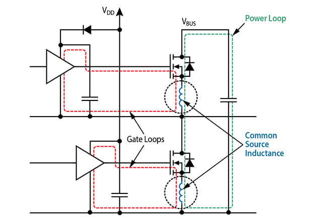
Figure 1: Schematic of a half-bridge power stage showing power and gate drive loops with common source inductance shown in dotted circles
Minimizing Parasitic Inductance
The minimization of all parasitic inductances is vital when considering the layout of high-speed power devices. It is not possible to reduce all components of inductance equally, and therefore, they must be addressed in order of importance, starting with common source inductance, then power loop inductance and, lastly, gate loop inductance.
For high-voltage PQFN (Power Quad Flat No lead) MOSFET packages, the need for a separate gate-return source pin is well known and is also implemented in high-voltage GaN PQFN structures [2,3]. When these separate pins are available, the gate drive loop and the power loop are separated within the package and extreme care must be taken in how they are connected externally.
The reduction in common source inductance comes at the expense of external source inductance, pushed outside the gate loop. This external inductance can lead to increased ground bounce due to the improved speed of the device once common source inductance is removed [4].
Enhancement-mode GaN transistors are available in a Wafer Level Chip-Scale Package (WLCSP) with terminals in a Land Grid Array (LGA) or Ball Grid Array (BGA) format. Some of these devices do not offer a separate gate-return source pin, but rather a number of very low inductance connections as shown in Figure 2. The total package inductance of these packages is often less than 100 pH. This greatly reduces all components of inductance, and thereby reduces all inductance-related problems. These LGA and BGA packages can be treated in the same way as ones provided with a dedicated gate return pin or bar by allocating the source pads closest to the gate to act as the “star” connection point for both the gate loop and power loop. The layout of the gate and power loops are then separated by having the currents flow in opposite or orthogonal directions as shown in Figure 2.
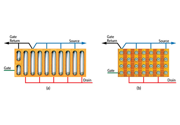
Figure 2: GaN transistors in LGA (a) and BGA (b) formats showing the direction of device current flow that minimizes common-source inductance
While minimizing the inductance of the individual elements that make up the loop (i.e. capacitor ESL, device lead inductance, and PCB interconnect inductance) is important, designers must also focus on minimizing the total loop inductance. As the inductance of the loop is determined by the magnetic energy that is stored within, it is possible to further minimize the overall loop inductance by using the coupling between adjacent conductors to induce magnetic field self-cancellation.
By interleaving the drain and source terminals on one side of the device, a number of small loops with opposing currents are generated that will decrease the overall inductance through magnetic field selfcancellation. This is not only true for the PCB traces shown in Figure 3(a), but also for the vertical solder connections and the interlayer connection vias shown in Figure 3(b). With multiple small magnetic field-cancelling loops formed, the total magnetic energy, and therefore inductance, is significantly reduced [5].
Figure 3: LGA GaN transistor mounted on a PCB showing alternating current flow (a) top view (b) side view
A further reduction in partial loop inductance is possible by bringing both drain and source currents out on both sides of the device from the centerline and duplicating the magnetic field cancellation effect. This works by reducing the current in each conductor, thus further reducing the energy stored, and the shorter current path yields a lower inductance.
Conventional Power Loop Designs
To see how power loop inductance minimization can be realized in an actual layout, two conventional approaches to power loops are presented for comparison. These two approaches will be called “lateral” and “vertical” respectively.
Lateral Power Loop Design
The lateral layout places the input capacitors and devices on the same side of the PCB in close proximity to minimize the area of the high-frequency power loop. The high-frequency loop for this design is contained on the same side of the PCB and is considered a lateral power loop, since the power loop flows laterally on a single PCB layer. An example of the lateral layout using an LGA transistor design is shown in Figure 4. The high frequency loop is highlighted in this figure.
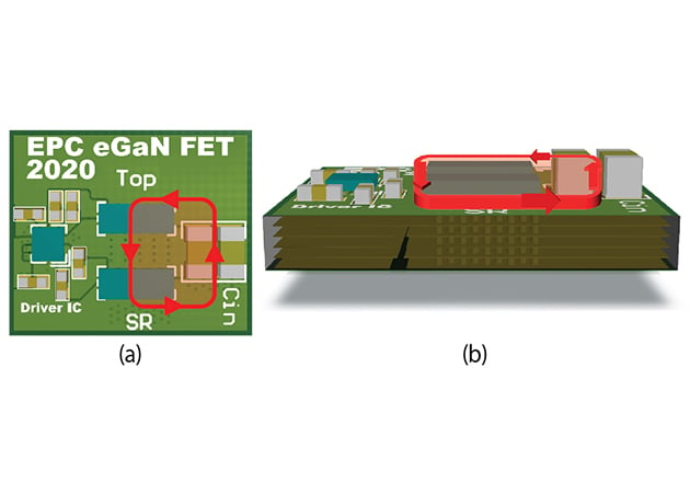
Figure 4: Conventional lateral power loop for LGA GaN transistorbased converter: (a) top view (b) side view
While minimizing the physical size of the loop is important to reduce parasitic inductance, the design of the inner layers is also critical. For the lateral power loop design, the first inner layer serves as a “shield layer.” This layer plays a critical role in shielding the internal circuits from the fields generated by the high-frequency power loop. The power loop generates a magnetic field that induces a current in the shield layer that flows in the opposite direction to the power loop. The current in the shield layer generates a magnetic field to counteract the original power loop’s magnetic field. The end result is a cancellation of magnetic fields that translates into a reduction in parasitic power loop inductance.
Having a complete shield plane in close proximity to the power loop yields the lowest power loop inductance for the lateral layout. This approach is strongly dependent on the distance from the power loop to the shield layer contained in the first inner layer [6]. As long as the top two layers are in close proximity, the high frequency loop inductance shows little dependence on total board thickness.
Vertical Power Loop Design
The second conventional layout, shown in Figure 5, places the input capacitors and transistors on opposite sides of the PCB, with the capacitors located directly beneath the devices to minimize the physical loop size. This is called a vertical power loop because the loop is connected vertically through the PCB using vias. The LGA transistor design of Figure 5 has the vertical power loop highlighted.
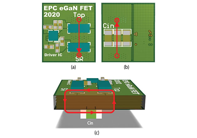
Figure 5: Conventional vertical power loop for LGA transistor-based converter: (a) top view (b) bottom view (c) side view
For this design, there is no shield layer due to its vertical structure. The vertical power loop uses a magnetic field self-cancellation method (with currents flowing in opposite directions) to reduce inductance, as opposed to the use of a shield plane.
For the PCB layout, the board thickness is generally much thinner than the horizontal length of the traces on the top and bottom sides of the board. As the board thickness decreases, the area of the loop shrinks significantly compared to the lateral power loop, and the current flowing in opposing directions on the top and bottom layers begins to provide magnetic field self-cancellation. For a vertical power loop to be most effective, the board thickness must be minimized.
Optimizing the Power Loop
An improved layout technique that provides the benefits of reduced loop size, has magnetic field self-cancellation, has inductance that is independent of board thickness, is a single-sided component PCB design, and yields high efficiency for a multi-layer structure, is shown in Figure 6. The design utilizes the first inner layer, shown in Figure 6(b), as the power loop return path. This return path is located directly beneath the top layer’s power loop, as shown in Figure 6(a). This positioning achieves the smallest physical loop area combined with magnetic field self-cancellation. The side view, shown in Figure 6(c), illustrates the concept of creating a low-profile magnetic field selfcancelling loop in a multilayer PCB structure.
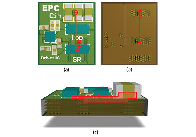
Figure 6: Optimum power loop for LGA transistor-based converter: (a) top view (b) top view of inner layer 1 (c) side view
This improved layout places the input capacitors in close proximity to the top device, with the positive input voltage terminals located next to the drain connections of the top transistor. The GaN devices are located in the arrangement as in the lateral and vertical power loop cases. The interleaved inductor node and ground vias are duplicated on the bottom side of the synchronous rectifier transistor.
These interleaved vias provide three advantages: • The interleaving of the vias with current flowing in opposing direction reduces magnetic energy storage and helps generate magnetic field cancellation. This results in reduced eddy and proximity effects, thus reducing AC conduction losses. • The vias located beneath the lower transistor reduces resistance and accompanying conduction losses during the transistor freewheeling period. • The vias reduce thermal spreading resistance, thus increasing efficiency and power handling.
The characteristics of the conventional and optimal designs are compared in Table 1. Lateral Loop Vertical Loop Optimal Loop Single-Sided PCB Capability Yes No Yes Magnetic Field Self-Cancellation No Yes Yes Inductance Independent of Board Thickness Yes No Yes Shield Layer Required Yes No No Table 1: Characteristics of conventional and optimal power loop designs
Impact of Integration on Parasitics
To further reduce the parasitic inductance of GaN transistor-based designs, monolithic GaN power stage integrated circuits are available [7]. In Figure 7, a block diagram and actual chip photo of a monolithic power stage GaN IC is shown. The experimentally measured efficiency of this monolithic integrated circuit, shown in Figure 8, is compared against a discrete circuit using eGaN® transistors with the same onresistance and driven by a uPI Semiconductor uP1966 Si half-bridge driver IC [7] in an optimal layout. The advantages of the reduced power loop and gate loop inductances in the GaN IC becomes clear as the overall efficiency gain from integration is significant at 1 MHz in a standard buck converter.
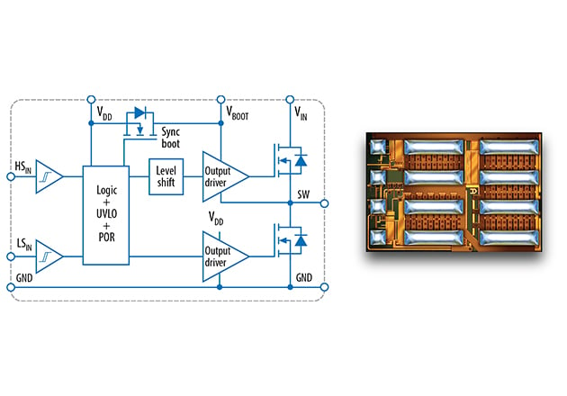
Figure 7: Block diagram for the monolithic power stage (a) and chip photo (b)
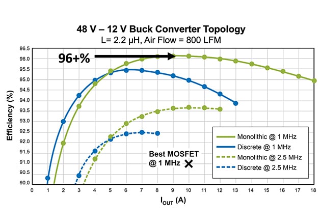
Figure 8: Efficiency comparison between the monolithic GaN power stage (green) and the externally-driven equivalent discrete GaN transistors (blue) solution in a 48 V – 12 V buck converter at 1 MHz (solid lines) and 2.5 MHz (dashed lines). The black “X” is the best reported MOSFET performance at 1 MHz.
Summary
An efficient circuit layout will minimize PCB area, reduce wasteful power dissipation due to slower switching speeds that are limited by parasitic inductances, and improve system reliability due to reduced voltage overshoot. Layout parasitics that are important when using GaN transistors were discussed; namely the common-source inductance, the high-frequency power loop inductance, and the gate loop inductance.
Several methods to minimize these performance inhibiting parasitics were reviewed, starting with the most basic single transistor through a complete monolithic GaN power stage IC. In future articles layout techniques discussed in this article will be built upon to show optimal thermal management systems design and how to create low EMI systems, all with modern chip-scale GaN transistors and ICs.
About the Author
Alex Lidow is CEO and co-founder of Efficient Power Conversion (EPC), former CEO of International Rectifier and is the co-inventor of the HEXFET power MOSFET, a power transistor. He has authored numerous peer-reviewed publications on related subjects, and received the 2015 SEMI Award for North America for the commercialization of more efficient power devices. Lidow was one of the lead representatives of the Semiconductor Industry Association (SIA) for the trade negotiations that resulted in the U.S. – Japan Trade Accord of 1986 and testified to Congress on multiple occasions on behalf of the industry.
References
- A. Lidow, M. de Rooij, J. Strydom, D. Reusch, and J. Glaser, GaN Transistors for Efficient Power Conversion, 3rd Edition, J. Wiley 2020.
- Zhou, L., Wu., Y.F., and Mishra, U. (2013) “True-bridgeless totem-pole PFC based on GaN HEMTs,” PCIM Europe 2013, pp. 1017–1022.
- Efficient Power Conversion Corporation, “eGaN FETs in high performance DC-DC conversion,” EDN Innovation Awards Conference and Awards, Shanghai, China, 2011, p. 28. Available from http://epc-co.com/epc/documents/presentations/EDN_Innovation_Conference_120111.pdf.
- Direct Energy, Inc., “The destructive effects of Kelvin leaded packages in high speed, high frequency operation,” Fort Collins, Colorado, Tech Note 9200-0002-1,1998. Available from www.directedenergy.com/index.php?option=com_joomdoc&task=document. download&path=ixysrf%2Fapplication-notes%2Fthe-destructiveeffects-of-kelvin-leaded-packages-in-high-speed-high-frequencyoperation.
- Krausse, G.J. “DE-Series fast power MOSFET, an introduction,” Directed Energy, Inc., Fort Collins, Colorado, Tech Note 9300- 002 Rev 3, 2002. Available from www.directedenergy.com/index. php?option=com_joomdoc&task=document.download&path=ixysrf %2Fapplication-notes%2Fde-series-fast-power-mosfet.
- Reusch, D. and Strydom, J. (16–21 March 2013) “Understanding the effect of PCB layout on circuit performance in a high frequency gallium nitride based point of load converter,” OT Twenty-Eighth Annual IEEE Applied Power Electronics Conference and Exposition (APEC), Long Beach, CA, pp. 649–655.
- A. Lidow, “The Ascent of GaN – Redefining Power Conversion with Gallium Nitride Integrated Circuits,” Bodo’s Power Systems, October 2020.
This article originally appeared in the Bodo’s Power Systems magazine.
Related Content