Facebook
 Google
 GitHub
 Linkedin
Analyzing the Options: EV Fast Charging Bi-Directional Topologies
Electric vehicle (EV) DC fast chargers currently under development have to meet more demanding specifications than today’s installed charger base. This article examines the options available to meet those challenges.
This article is published by EE Power as part of an exclusive digital content partnership with Bodo’s Power Systems.
Electric vehicle (EV) DC fast chargers currently under development must meet more demanding specifications than today’s installed charger base. This stems from two market pressures: First, to provide for faster charging of the higher-capacity batteries embedded in the latest EVs and, second, to enable bi-directional power flow, supporting new vehicle-to-grid (V2G) and vehicle-to-building (V2B) applications – technology that will help balance the power grid as more energy is generated from fluctuating sources such as wind and solar power.
Charger manufacturers can build flexibility into their designs by implementing DC fast chargers as modular building blocks: multiple modules can be connected in parallel to scale up the power output to as high as 300 kW. This means that when multiple modules are stacked in a charger’s enclosure, the power density of the module becomes a key issue, as does thermal management.
To address these challenges, EV charger manufacturers have turned to silicon carbide (SiC) power switches, which can switch faster than equivalent silicon MOSFETs or IGBTs with much lower switching losses. This enables smaller magnetic components, resulting in higher system power density. SiC technology also answers the thermal problems of high-density power designs because of its higher efficiency and toleration of higher operating temperatures than silicon devices, enabling a smaller heat sink while reducing thermal stress on the system’s components.
A few semiconductor manufacturers have the technical capability and manufacturing capacity to supply SiC devices in volume to charger manufacturers. Leading the group are Infineon, onsemi, and STMicroelectronics. Many EV charger designers will look to these companies to provide reference design boards to evaluate the performance of various SiC power switches and assess their suitability for their application.
These reference designs provide implementations of some of the most appropriate topologies for bi-directional DC fast chargers, both at the PFC and DC/DC converter stages. Understanding these topologies, and their benefits and drawbacks, will help the designer work out which best fits the requirements of their application. Let’s look first at the choice of topologies for an EV charger’s active front-end PFC stage.
Active Front-End PFC Stage of a DC Charger Module
The AC/DC stage converts a (normally) three-phase input in the range 380 V-415 V AC into a stable DC link voltage of around 800 V. All the topologies examined in this article are for bi-directional systems, so the conversion will also go the other way, from DC to AC.
SiC devices are particularly well suited to bi-directional converters based on a half-bridge configuration. Usually, bi-directional systems perform repetitive hard commutation. In this case, a silicon power switch’s long reverse-recovery time at the device’s body diode will lead to high power dissipation, low efficiency, higher thermal stress, and lower system reliability. So a bi-directional converter requires low or even zero reverse-recovery time, a feature of SiC MOSFETs (see Figure 1).

Figure 1. Low body diode reverse-recovery time is essential in bidirectional converters, which have a half-bridge configuration and are exposed to repetitive hard commutation. Image used courtesy of Bodo’s Power Systems [PDF]
There are three topologies worth considering for the active front-end PFC stage of three-phase bi-directional DC chargers:
- Two-level PFC
- Three-level neutral point clamped (NPC)/active NPC (ANPC)
- Three-level T-type NPC

Figure 2. The two-level PFC topology. Image used courtesy of Bodo’s Power Systems [PDF]
Two-Level PFC Topology
The six-switch boost-type rectifier of the two-level PFC topology is a very simple circuit that is easy to control (see Figure 2). It facilitates bi-directional power flow and can achieve a high power factor with reasonable efficiency. Compared to a three-level topology, it results in a lower component count and an easier PCB layout.
On the other hand, it requires switches with a high voltage rating to block the entire DC link voltage. For example, an 800 V DC application requires a SiC MOSFET with a 1,200 V blocking capacity.
An additional drawback of this topology is the bulky filter inductor, which is required to minimize the total harmonic distortion (THD) at the input current. Three-level topologies do not need so much inductance and enable lower power density.
Another factor to consider is the high peak-voltage stress, which compromises the lifetime of the semiconductor and other passive devices.
Finally, the converter’s EMI performance is substantially lower than the multi-level PFC topologies described below.
Three-Level NPC/ANPC PFC Topology
In the three-level NPC/ANPC topology, each switch only needs to block half the bus voltage, so MOSFETs with a lower voltage rating can be used, and the voltage stress on devices is much lower (see Figure 3). This means that this topology can be easily scaled across multiple platforms for implementation with SiC, GaN, and silicon power switches to meet the needs of applications with different power, cost, and efficiency requirements.
In an 800 V application, 600 V-rated MOSFETs may be used. As well as offering lower switching losses than 1,200V MOSFETs, 600 V MOSFETs can support much faster switching frequencies.
In the NPC topology, lower ripple is observed in the output current, and the output-voltage transient is 50% lower. This reduces the requirement for filtering and isolation and allows for a smaller filter inductor. The design can achieve higher power density with less inductance needed to regulate THD in the current waveform. This multi-level converter topology’s output voltages also suffer very low disturbance, which minimizes the dv/dt stresses across devices and improves EMI performance.
While the NPC topology offers lower switching losses and higher efficiency at switching frequencies higher than 50 kHz than the two-level PFC, it does require more switches, and each switch needs its own gate-drive circuit. This means that control is more complex, and the bill-of-materials (BoM) cost is higher.

Figure 3. Three-level NPC PFC topology. Image used courtesy of Bodo’s Power Systems [PDF]
In addition, this topology uses both active semiconductor switches and diodes, and the resulting unsymmetrical distribution of losses across the power stage can make thermal management difficult. Some designers prefer a more symmetrical distribution of losses, so replace the diodes of the NPC topology with active switches in an ANPC converter (see Figure 4).
It is useful in both NPC and ANPC topologies that the reduced blocking voltage across all switches means that high-efficiency gallium nitride (GaN) switches can improve efficiency and power density.

Figure 4. Three-level ANPC PFC topology. Image used courtesy of Bodo’s Power Systems [PDF]
Three-Level T-Type NPC PFC Topology
In three-level T-type NPC PFC converters, the conventional two-level voltage source converter (VSC) topology is extended with an active, bi-directional switch to the DC link midpoint (see Figure 5). For 800 V DC link voltages, 1,200 V IGBTs/diodes would normally operate on the high and low sides of each phase, as the full voltage has to be blocked. But in the T-type configuration, the bi-directional switch to the DC link midpoint only needs to block half of the voltage. This means it can be implemented with lower-voltage devices, for example, two 600 V IGBTs that include antiparallel diodes.
Due to the reduced blocking voltage, the middle switch generates very low switching losses and acceptable conduction loss. Unlike the three-level NPC topology, the T-type NPC topology does not connect devices in series that must block the whole DC link voltage.
In the NPC topology, switching transitions made directly from a positive to a negative DC link voltage, and vice versa, are usually avoided, as they might cause an uneven share of the voltage to be blocked momentarily when both FETs connected in series turn off simultaneously. This undesirable effect cannot occur in the Ttype topology. Therefore it is not necessary to implement low-level routines which prevent such transitions or provide for transient voltage balancing across series-connected IGBTs.
Another benefit of using single 1,200 V devices to block the full DC link voltage is reduced conduction losses. Whenever the output is connected to positive or negative, the circuit is exposed to the forward voltage drop of only one device; in the NPC topology, two devices are always connected in series. This considerably reduces conduction losses, making the T-type topology valuable in applications that switch at a low frequency.
Overall, conduction losses are significantly lower than those of the NPC topology, but switching losses are high because of the devices that block the full DC link voltage. So the T-type rectifier is best suited for applications switching at up to 50 kHz, while the NPC topology performs better at frequencies higher than 50 kHz.

Figure 5. Three-level T-type NPC PFC topology. Image used courtesy of Bodo’s Power Systems [PDF]
Table 1 compares the advantages and drawbacks of the three PFC stage topologies described above.
Table 1. Summary of features of PFC topologies.
|
|
Two-level PFC |
Three-Level NPC |
Three-level ANPC |
Three-level T-type NPC |
|
Power Density |
Low |
Higher |
Higher |
Highest |
|
Efficiency |
Low |
Very high at high frequencies |
Highest |
High |
|
Conduction Loss |
Low |
High |
High |
Mid |
|
Switching Loss |
High |
Low |
Low |
Mid |
|
Peak Voltage Stress |
High |
Low |
Lowest |
Low/(high blocking voltage) |
|
Cost |
Low |
High |
Highest |
Mid |
|
Control |
Easy |
Mid |
Mid |
Mid |
|
Input Inductor |
Large |
Small |
Small |
Small |
|
Number of Active Switches |
6 |
12 |
18 |
12 |
|
Number of SiC Diodes |
0 |
6 |
0 |
0 |
DC/DC Converter Stage of a DC Charger Module
The DC/DC stage is the galvanic isolated converter that converts the incoming DC link voltage of 800 V to a regulated DC output voltage for charging the EV battery (bypassing the vehicle’s onboard charger, which is used only when connecting to an AC charger).
The topology for the bi-directional DC/DC stage can be implemented in one of two ways:
- Dual active bridge
- Dual active bridge in CLLC mode
Dual Active Bridge Topology
The dual active bridge (DAB) converter consists of a full bridge with active switches on both the primary and secondary sides, connected via a high-frequency transformer (see Figure 6). Because of the inherently lagging current in one of the bridges, the current discharges the output capacitance of the switches of one bridge at a time. While the secondary side switches are discharged, some switches on the primary side enable zero-voltage switching turn on. Loss-less capacitive snubbers can also be used across the switches to reduce turn-off losses.
The main advantages of this converter topology are:
- Bi-directional capability, which is achieved by controlling the phase angle between the two bridges
- Modularity, which allows for it to be scaled to higher power levels

Figure 6. Dual active bridge DC/DC converter topology. Image used courtesy of Bodo’s Power Systems [PDF]
In single-phase shift modulation, the DAB topology is simple to control. However, the control scheme becomes complex for extended, dual- or triple-phase shift modulation. This topology may cover a wide range of battery voltages with single-phase shift modulation, but circulating currents in the transformer rise to elevated levels, greatly reducing efficiency.
However, with advanced modulation schemes such as triple-phase shift modulation, the converter can theoretically perform zero-voltage switching over the entire operating range. The ratio of output power to the transformer’s KVA rating is high in this topology. The output capacitance required to handle ripple currents is also low.
Overall, this converter is ideal for applications in which power density, cost, weight, isolation, and reliability are critical factors because of its range of attractive features:
- Relatively low component count
- Soft-switching commutation
- Low cost
- High efficiency
It is worth noting, however, that the DAB converter often requires an additional shim inductor to support zero-voltage switching: this increases the size of the circuit and reduces power density.
DAB Topology in CLLC Mode
The CLLC circuit configuration performs all the functions of the classic LLC but has the advantage that using active switches across the secondary side enables bi-directional power transfer (see Figure 7).
This converter operates in zero-voltage/zero-current switching mode, resulting in high efficiency. When there is room to vary the bus voltage by a margin of 10%, this converter can cater to a widely varying battery voltage while maintaining good efficiency. With a fixed bus voltage, however, this topology has a very limited range of operation.
The presence of capacitors on both the primary and secondary sides eliminates the risk of saturation of the transformer’s core.
The DAB converter in CLLC mode is best suited to AC/DC onboard chargers. It can be used at power levels higher than onboard chargers handle – up to 15 kW. But scaling to higher power levels and paralleling can be difficult, as it requires a highly symmetrical tank structure and synchronization of multiple modules – a difficult task.

Figure 7. DAB topology in CLLC mode. Image used courtesy of Bodo’s Power Systems [PDF]
The DAB and DAB in CLLC mode topologies are commonly used in 800 V isolated DC/DC converters. The voltage conversion ratio controls the connection for the converter terminals, which affects the breakdown voltage rating required for the switches: a high-voltage converter could be connected in series or in parallel in one terminal while another remains connected in parallel. This means that there are four possible configurations for the topology’s connections.
Two examples of the DAB topology in CLLC mode are shown: Figure 8 shows a series input configuration, and Figure 9 a parallel input configuration for an 800 V bus voltage with a wide output-voltage range of 200 V to 1 kV.
The advantage of the series-input full-bridge CLLC is its narrow resonant-frequency range over a wide output-voltage range, resulting in lower switching losses; here, a 650 V device could be used. But this calls for more complex control of the DC bus capacitor voltage in series on the DC bus side. In addition, to achieve a given efficiency, a device with lower on-resistance is required than in a single full bridge using 1,200 V devices.
The advantage of the parallel-input full-bridge DAB converter in CLLC mode is that, for a given efficiency, the circuit can use devices with a higher on-resistance, while the control scheme is easier. A wide resonant-frequency range is required to support a wide output-voltage range.

Figure 8. DAB converter in CLLC mode with series input. Image used courtesy of Bodo’s Power Systems [PDF]

Figure 9. DAB converter in CLLC mode with parallel input. Image used courtesy of Bodo’s Power Systems [PDF]
The advantages and drawbacks of the two DC/DC stage topologies are shown in Table 2.
Reference Designs Accelerate DC Charger Circuit Implementation
The leading SiC MOSFET manufacturers supply reference designs that provide a blueprint for new high-power DC charger designs, in part or whole.
The STMicroelectronics STDES-PFCBIDIR 15 kW bi-directional PFC stage converter implements the T-type NPC topology (see Figure 10). Digitally controlled, it converts between 400 V AC and 800 V DC. Efficiency is almost 99%. ST has optimized the passive components for both size and cost, and the converter offers high power density.
Table 2. Summary of the features of two DC/DC stage topologies.
|
|
DAB |
DAB in CLLC mode |
|
Peak Device Stress |
Low |
High |
|
Switching Frequency |
High |
Very High |
|
Control |
PWM (simple) |
Frequency (moderate) |
|
Wide Battery Voltage Range, Fixed Bus Voltage |
Yes (with reduced efficiency) |
Limited range |
|
Input RMS Currents |
Low |
High |
|
Conduction Losses |
Low |
Medium |
|
Turn-on Switching Loss |
ZVS |
ZVS |
|
Turn-off Switching Loss |
High (device turn off at peak leakage inductor current value) |
Low (primary-side turn-off decided by magnetizing inductor current, secondary-side turn-off is zero to ZCS) |
|
Total Losses |
Medium |
Low |
|
Efficiency |
High |
Very High |
|
Paralleling Modules |
Easy |
Difficult |
|
Number of Active Switches |
8 |
8 |

Figure 10. The STDES-PFCBIDIR PFC reference design from STMicroelectronics is notable for its high efficiency and power density. Image used courtesy of Bodo’s Power Systems [PDF]
A pairing of the STDES-PFCBIDIR with ST’s 25 kW STDES-DABBIDIR provides a complete solution for a bi-directional EV charger. The STDES-DABBIDIR implements the DAB topology switching at 100 kHz with a SiC MOSFET power module in an ACEPACK 2 package (see Figure 11). An STM32G474RE MCU performs digital control. Adaptive modulation techniques manage soft-switching operations, which respond to variations in load and voltage.
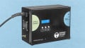
The Infineon REF-DAB11KIZSICSYS is a bi-directional DC/DC converter stage that implements the DAB topology in CLLC mode (see Figure 12). It provides an output of up to 11 kW at 800 V, higher than 97% efficiency.
Based on the IMZ120R030M1H CoolSiC MOSFETs driven by the Infineon 1EDC20I12AH gate driver, the board combines high power density and reliability at low cost.

Figure 11. The STDES-DABBIDIR DC/DC converter reference design board has a power rating of 25 kW. Image used courtesy of Bodo’s Power Systems [PDF]

Figure 12. The Infineon REF-DAB11KIZSICSYS reference design board has an 11 kW output rating. Image used courtesy of Bodo’s Power Systems [PDF]

Image used courtesy of Bodo’s Power Systems [PDF]

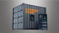
Figure 13. The REF-EV50KW2SICKIT from Infineon implements a complete DC/DC fast charger. Image used courtesy of Bodo’s Power Systems [PDF]
Infineon has also developed a complete DC/DC charger reference design, the REF-EV50KW2SICKIT, due for imminent release in March 2023. This 50 kW DC charger sub-unit is intended as a module in stacked high-power charging systems (see Figure 13).
The design achieves a power factor higher than 0.95 and maximum efficiency of 96%.
On release, Infineon will offer fully assembled boards that fit into a 19” 4U rack. A power control card plus software with GUI will also be available.
Another complete DC/DC charger design is supplied by onsemi. The SEC-25KW-SIC-PIM-GEVK is a 25 kW charger that implements the two-level PFC and DAB topologies (see Figure 14).

Image used courtesy of Bodo’s Power Systems [PDF]

Figure 14. SEC-25KW-SIC-PIM-GEVK reference design from onsemi is a 25 kW DC/DC charger. Image used courtesy of Bodo’s Power Systems [PDF]
The SEC-25KW-SIC-PIM-GEVK features multiple NXH010P120MNF1 half-bridge SiC modules, which have a breakdown-voltage rating of 1,200 V. Notable for their very low on-resistance of 10 mΩ and low parasitic inductance, these SiC modules substantially reduce conduction and switching loss. Conversion operations are controlled by a powerful universal controller board based on a Zynq®-7000 SoC FPGA. The output-voltage range is 200 V to 1,000 V, and efficiency is up to 96%.
Multiple SEC-25KW-SIC-PIM-GEVK boards can be stacked together in a single cabinet to supply the output power required by the application.
Optimizing Fast-Charging Features
The choice of topologies in the PFC and DC/DC converter stages of bi-directional EV fast chargers allows the designer to optimize for size, cost, efficiency, output power, component count, and ease of control.
The availability of high-performance reference designs from the leading SiC device manufacturers gives designers a head start in implementing some of these topologies.
This article originally appeared in Bodo’s Power Systems [PDF] magazine.