Facebook
 Google
 GitHub
 Linkedin
How Does Flyback Synchronous Rectification Affect EMI?
This article highlights Monolithic Power Systems flyback adapter design with synchronous rectification (SR) as different from conventional set-ups with a Schottky diode.
Due to the rapid development of mobile devices in the last decade, cell phone applications have expanded into every aspect of society. In day-to-day life, few people leave their cell phone, even for a few minutes. As a result, high battery capacity and fast charging speed has become one of the most critical features for cell phones, and the demand for adapters with higher power ratings and higher power density has increased exponentially.
The old 5V/1A output specification has become obsolete. New designs are generally above 2A, with up to a 20V output. Most of the cell phone market leaders (e.g. Huawei, Oppo, and Vivo) have been promoting their high-power adapters as standard in-box accessories for years, and the market feedback has been very positive. In Apple’s 2020 autumn press release, they abandoned their standard 5V/1A in-box adapter, which has stimulated another boom for the demand of aftermarket high-power adapters.
Flyback topologies are still the most popular solution for these highpower mobile phone adapters. However, synchronous rectification (SR), which can be accomplished through SR MOSFETs, is one of the major evolutions in adapter design due to this new market trend. Synchronous rectification has become the mainstream solution on the secondary side of adapters, replacing the conventional Schottky diode.
Synchronous Rectification Basics
Synchronous rectification solutions utilize a MOSFET for output current rectification. Compared to the relatively fixed forward voltage drop of a diode, a MOSFET’s voltage drop is proportional to the current and turn-on resistance (see Figure 1). A MOSFET significantly impacts the conduction power loss of the rectification. In other words, by selecting an SR MOSFET with an ideal turn-on resistance, an SR solution can achieve better efficiency and thermal performance than a conventional diode solution, which is the most critical requirement for high-power adapter designs.
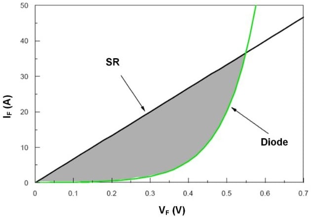
Figure 1: Difference in I-V Characteristics Between MOSFET and Diode
In a conventional flyback converter application with a Schottky diode on the secondary side, it is well known that the switching characteristic of the diode (especially the reverse recovery current) has a significant effect on the EMI performance. Therefore, it must be carefully dealt with in practical applications. After replacing the diode with a synchronous rectification MOSFET, the situation is completely different, because the MOSFET does not have a theoretical reverse recovery effect.
However, this does not necessarily mean that a synchronous rectification solution has fewer EMI problems. On the contrary, designers should pay more attention to how they design flyback solutions with SR, especially in regards to EMI noise source and the coupling path.
Synchronous Rectification Impact on the EMI Noise Source Amplitude To understand the impact on the EMI noise source, SR operation principles must be discussed in greater detail. Most controllers drive the SR MOSFET based on the direct detection of the drain-source voltage (VDS), as this does not require communication with the primary side and reduces the total BOM cost. Figure 2 shows that there are usually two thresholds to control the SR MOSFET when it turns on and off. They are both negative voltage thresholds to guarantee that the SR MOSFET is always securely turned off when it is reversely biased.
As a result, there are short periods of body diode conduction at both ends: just before the device turns on, and after the SR MOSFET turns off. The timing control is critical for SR controllers, as these two periods can introduce extra conduction loss (with longer times being worse). In addition, but if the turn-off time is too long, it may lead to a severe reverse recovery current after the SR turns off, because of the poor characteristics of the MOSFET’s body diode.
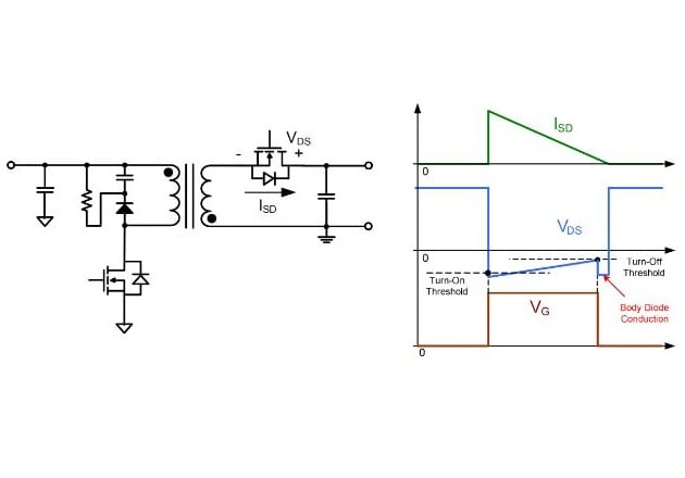
Figure 2: Basic Operation Principle of Flyback SR Solution
Figure 3 shows how the reverse recovery current of the body diode went up to 9A because of the SR’s early 400ns turn-off, which then led to an 80V high-voltage spike due to the leakage inductance. It is commonly understood that EMI problems are closely related to the pulse amplitude and the slew rate of the noise source. This corresponds to a stronger EMI noise source on the secondary side of the flyback converter.
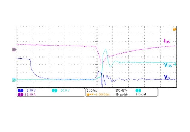
Figure 3: High-Spike Current and Voltage Caused by SR Early Turn-Off
A similar problem occurs if the SR turn-off is too late. Figure 4 shows the results if the SR is turned off after the current is reversed due to the propagation and driving delay. This leads to a short shoot-through period because the primary and the secondary MOSFET turn on at the same time. As a result, the negative current rises to a high 10A amplitude. This leads to an 87V high-voltage spike after the SR MOSFET turns off.
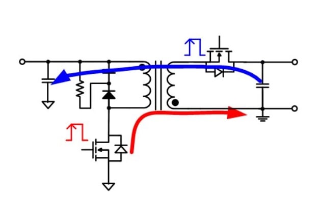
To mitigate these issues, it is vital that the timing of the SR turn-on and turn-off are both well-controlled. Figure 5 shows the MP6908, a, SR controller with intelligent fast turn-off from Monolithic Power Systems (MPS). As the market leader of flyback synchronous rectification controllers, the MP6908 implements the most advanced SR control scheme currently available in the industry. The precise and sophisticated signal process, proprietor gate voltage regulation, and super-fast turn-off speed enable optimized synchronous rectification timing control.
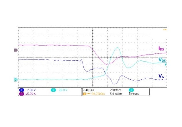
Figure 4: High-Spike Current and Voltage Caused by SR Turn-Off
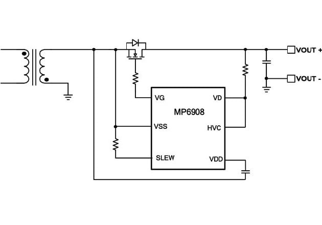
Figure 5: Typical Application of MPS’s MP6908 in a Flyback Solution
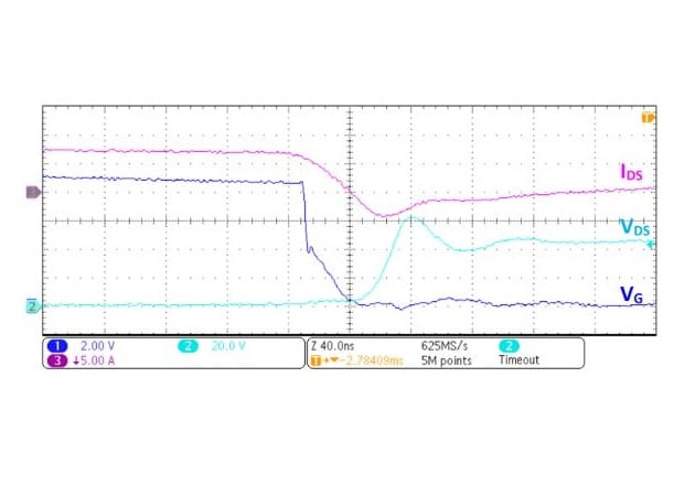
Figure 6: Low-Spike Current and Voltage with the MP6908’s Optimized Timing Control
(a)
(b)
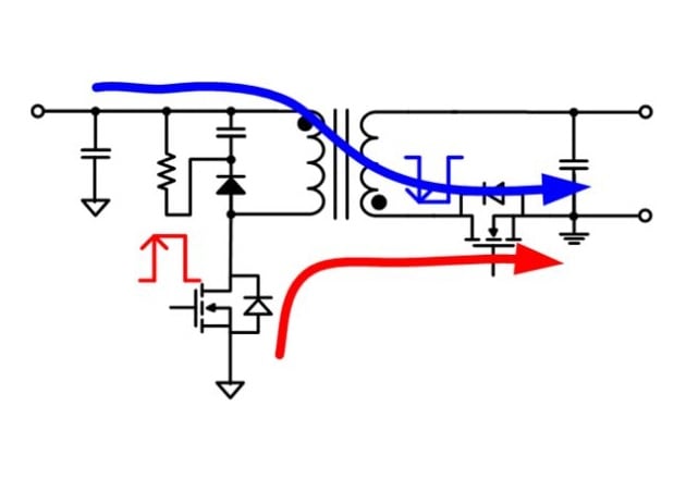
Figure 7: Comparison between High-Side SR and Low-Side SR (a) CM Noise Coupling Path with Low-Side SR (b) CM Noise Coupling Path with High-Side SR
The MP6908 demonstrates that by controlling the turn-on and turn-off timing, there is a relatively low spike in both current and voltage (4A and 62V, respectively) (see Figure 6). This results in reduced EMI noise.
SR’s Impact on the CM Noise Cancellation Effect
In many flyback synchronous rectification solutions on the market, it is recommended to place the SR on the low side of the secondary side winding, because it is much simpler for the SR controller to get biased power directly from the output. However, the conventional Schottky diode is always placed on the high side, which implies there is some benefit to this location. In fact, there is a major difference between a high-side and low-side SR placement in flyback converters, regarding the common mode (CM) noise cancellation effect (see Figure 7).
Each side (primary and secondary) of the flyback converter has one main CM noise source, and that is where the switching device and the transformer winding are connected together (see Figure 7).
Figure 7a shows when the synchronous rectifier is placed at the low side. The primary CM noise source and the secondary CM noise source are on the winding ends with different magnetic polarities. As a result, the switching directions of the two noise sources are always in the opposite direction. Since the two noise sources are on opposite sides of the transformer, the CM noise each creates has an additive effect, thus making more noise.
Figure 7b shows when the SR is placed at the high side, and the two noise sources are on the winding ends with the same magnetic polarity. In this scenario, the switching directions of the two noise sources are always in the same direction, and there is a cancellation effect between them.
Based on these analyses about CM noise coupling, the high-side SR set-up has an obvious advantage over the low-side placement in terms of EMI performance. It is also very common to get a difference of 3dB or more between the high-side and low side set-ups in practical application designs.
Conclusion
Flyback adapter design with SR is different from conventional set-ups with a Schottky diode. When adopting an synchronous rectification solution, the two main expectations are improved efficiency and thermal performance. However, there are other aspects to consider, such as EMI performance.
With a well-controlled flyback synchronous rectification solution, designers can achieve better performance, a lower power device rating, higher product reliability, and minimize EMI noise. At the same time, devices like the MP6908 from MPS integrate an internal high-voltage regulator that can provide self-biased power without any external circuitry. When paired with a high-side SR set-up, these systems can also reduce BOM costs while developing more sophisticated adapter designs that are free of EMI issues.
This article originally appeared in Bodo’s Power Systems magazine.
About the Author
Siran Wang is a Technical Marketing and Application Engineering Manager at Monolithic Power Systems. He has PhD in Electrical Engineering from Zhejiang University, and he has more than 9 years working experience in the power management IC industry, with expertise in AC/DC and lighting applications.