Facebook
 Google
 GitHub
 Linkedin
950V IGBT and Diode Technology Integrated in a Low Inductive ANPC Topology
This article highlights Active Neutral-Point clamped (ANPC) topology. This combination brings the power density of 1500 VDC PV string inverter to the next level, which leads to a further reduction of LCoE.
In the past two years, with the booming of the global PV market, and the benefits of a lower levelized cost of energy (LCoE), 1500 VDC photovoltaic systems have been established as mainstream. In the meantime, the string inverter solution is also becoming increasingly popular owing to its continuously enhanced power density, flexibility, and simplified maintenance.
Investigated ANPC Topology
To support this market trend, Infineon has developed the new, low-inductive Easy 3B package and a special 950 V IGBT and diode technology. Together with the active neutral-point clamped (ANPC) topology, this combination brings the power density of 1500 VDC PV string inverter to the next level, which leads to a further reduction of LCoE.
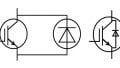
Figure 1 shows a typical ANPC topology used in solar inverters. SHeading 2ix subsystems are used and each subsystem consists of an IGBT (T1 to T6) with an antiparallel diode (D1 to D6). VDC is symmetrically applied from DC+ to N and from N to DC-. The investigated ANPC

Figure 1: Schematic drawing of an ANPC topology with fast-switching devices and low-static loss devices in the subsystems 1 to 4 and 5 to 6, respectively. The solid and dotted green lines indicate the investigated commutation path
topology uses fast-switching devices in the subsystems 1 to 4, and low-static loss devices in the subsystems 5 and 6. A comprehensive discussion and explanation of ANPC topologies and the relevant commutation paths is provided in Ref. [1, 2].
In active power, e.g., positive output voltage and positive output current, the solid and dotted green lines in figure 1 indicate the typical commutation path. For clarity, T1 commutates with D2, whereas T5 is continuously in an ON-state. Consequently, one main commutation path for active-power operation is between DC+ and N and/or N and DC-. Therefore, parasitics should be minimized in these paths by design measures to ensure optimized performance.

Figure 2: Trade-off diagram of 650 V, 950 V, and 1200 V MPT IGBT technologies. Static and dynamic values are provided at TJ=150°C and with VDC=2/3∙VCES. As a reference, 650 V and 1200 V state-of-the-art, 4th generation IGBTs are indicated as well
New 950 V technology for solar applications The new 950 V IGBT technology is based on a micro-pattern trench (MPT) cell design, which is well known from the 650 V TRENCHSTOP™ 5 and 1200 V TRENCHSTOP™ 7 IGBTs [3, 4, 5]. In order to meet the specific requirement of each subsystem in ANPC topology and to optimize the efficiency of the system, two independent device performances were developed: a fast-switching IGBT (S7) with moderate static losses, but significantly reduced dynamic losses, and a low-static loss optimized IGBT (L7). The new 950 V diode is based on the well-known 650 V RAPID technology and provides adequate softness, cosmic-ray robustness, but also low dynamic losses.
Figure 2 shows the trade-off diagram of 650 V, 950 V, and 1200 V MPT technologies. All values are provided at a junction temperature (TJ) of 150°C, nominal current, and a DC-link voltage (VDC) of 2/3 of the corresponding blocking voltage VCES. As one can see, the 650 V MPT technology offers very fast-switching devices (H5) with higher static losses as well as static loss optimized devices (L5). The 1200 V MPT technology (T7) combines low static losses with moderate dynamic losses compared to 1200 V T4. At any rate, due to the blocking capability of 1200 V, T7 provides larger (by nearly factor 8) dynamic losses than S5, although both offer comparable collector-emitter voltages (VCE) at nominal current (Inom). Consequently, the 950 V MPT technology closes this performance gap.
L7 provides approximately 50 percent higher dynamic losses than T7 but at significantly lower static losses. S7 shows only a third of T7’s dynamic losses at moderate static losses. One should keep in mind that current density decreases with increasing blocking voltage In the case of L7 and S7, the current density is approximately 50 percent higher compared to T7. Thus, if equal chip areas are used in a power module, the performance benefits of 950 V IGBTs becomes even more pronounced with respect to 1200 V IGBTs. Additionally, comparing L7 and S7 to the state-of-the-art 1200 V T4 and 650 V E4, emphasizes the benefits directly related to the MPT concept and technology used.

Figure 3: Turn-off waveforms (left-hand side) and turnon waveforms (right-hand side) of L7, S7, and T7 for IC= Inomand IC=0.1 ∙ Inom, respectively, with VDC=600 V at TJ=25°C. The tables contain characteristic parameters
In the following, the focus is on L7, S7, and T7. Figure 3 displays turn-off and turn-on waveforms of L7, S7, and T7. For turn-off, S7 provides the most aggressive switching behavior, i.e., the highest switching slope (dv/dt) and peak voltage VCE, peak. Focusing on S7, VCE, peak are close to its maximum value. L7 and T7 are very soft and do not reach critical values. For turn-on, all devices provide comparable switching performance. S7 might achieve lower switching losses and higher dv/dt values if the gate resistor (RG) is reduced additionally.
Optimized Power Module for 1500V Solar Applications
As discussed in Ref. [6], an optimized power-module design is mandatory to achieve best performance in the final system. For this purpose, the following steps were taken to develop an optimized power module for 1500 V solar applications:
First, the main commutation paths of the ANPC topology were identified, as depicted in figure 1.
Second, the power terminals were positioned close to each other in a parallel-plate design to minimize stray inductance between DC+ and N and N and DC. The positions of DC+, N, and DC- are indicated in figure 4. The output terminals are situated opposite the input terminals allowing a simplified PCB design.
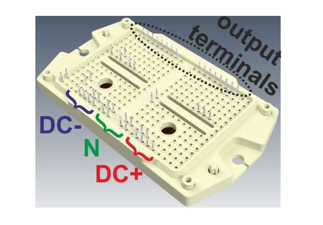
Figure 4: Easy3B package with the corresponding pinout of a 950 V based ANPC topology
Third, the internal layout was defined in such a way that only very small commutation loops occur on the substrate level for the critical computation paths. Commutation paths between the module substrates are avoided.
Fourth, a very low inductive and symmetric power module was developed using the novel baseplate-less Easy3B package. Hence, a module-stray inductance of only 15 nH has been achieved on the same footprint as for two conventional Easy2B packages. In addition, the Easy3B package provides a reduced thermal impedance com-pared to Easy1B and Easy2B.
And finally, the 950 V IGBT and diode technology has been implemented in this power-module design. Thus, an ANPC topology optimized for 1500 V solar inverters with a nominal current of 400 A is fully integrated in a single power module.
The performance of the power module is evaluated using the 1500 V ANPC topology seen in figure 1. S7 and L7 are implemented in the subsystems T1 to T4 and T5 to T6, respectively. Whereas T2 and T3 provide an Inom of 200 A, all other IGBTs have an Inom value of 400 A. With respect to the diode, two main scenarios are analyzed. In the first one, 200 A RAPID diodes are integrated in all subsystems. In the second one, 1200 V SiC Schottky diodes with Inom=60 A replace the RAPID diodes D2 and D3. An ANPC topology with T7 and EC7 is used as a reference, and the comparison is performed for the active-power commutation path. In all cases, a maximum increase of the average module temperature of 30 K is presumed, which consequently limits the solution’s usability.
Figure 5 shows the maximum achieved output current Iout versus switch-ing frequency fSW with 1200 V applied between the terminals of DC+ and DC-. The solid lines represent Iout of the reference and the two L7/S7-based scenarios mentioned above. All three solutions provide identical nominal currents. At very low fSW, the T7/EC7 solution offers up to 15 percent higher Iout than the two L7/S7 variants. At typical fSWabove 20 kHz, this benefit is reduced to approximately 7 percent. It is important to mention that only the significantly lower power density of the T7/EC7 solution leads to this imaginary Iout benefit. If an equal power density, i.e., identical chip areas of L7, S7, and RAPID diodes, is used, the situation changes. The dashed lines visualize this.

Figure 5: Iout versus fSW for different variants and power densities at equal thermal boundary conditions. Inset: System efficiency versus fSW for different variants and power densities at the corresponding Iout.
It becomes clear that L7/S7 with RAPID diode and L7/S7 with SiC diode now provide up to 40 percent and 75 percent increased Iout, respectively. Even for fSW in the range of 20 to 40 kHz, Iout is larger than the T7/EC7 reference by a minimum of 10 percent and maximum of 26 percent. These findings are not surprising, as T7 and EC7 are optimized for general-purpose drives, and thus, lower switching frequencies. Therefore, the benefits of L7 and S7 come to the fore if faster switching is required as in solar applications.
The inset of figure 5 displays system efficiency versus fSW for the corresponding maximum Iout. All solutions provide a system efficiency of a minimum of 99.2 percent. At any rate, L7/S7-based solutions offer a minimum 0.05 percent up to 0.3 percent higher system efficiency than a T7-based one. One should keep in mind that the slightly lower system efficiency for L7/S7 with larger chip sizes (dashed lines) is accompanied by significantly higher Iout when compared to the L7/S7-based solution with Inom=400 A (solid lines). Although system efficiency is marginally smaller, Iout is 25 percent to 35 percent enhanced at fSW=20 kHz.
Summary
This article presents the new 950 V technology and its inherent design options, and compares them to existing 1200 V technologies. The implemented cell design enabled the development of a static-loss-optimized IGBT (L7) and a fast-switching IGBT (S7). Compared to state-of-the-art 1200 V IGBTs, significantly reduced static losses and/or improved switching performance were achieved, as well as better system performance. With the help of a comprehensive analysis on the interaction of power-module designs and ANPC topology [6], the critical commutation paths and system-limiting factors were identified.
Based on this optimized power-module design, a fully integrated ANPC topology with a nominal current of 400 A for 1500 V solar inverters was presented. The ANPC topology was implemented in the recently introduced Easy3B package, which enables the implementation of a module-stray inductance of only 15 nH. This power-module design together with the presented 950 V technology offers two options in the application. On the one hand, the identical output power was achieved at a massively smaller footprint if a given 1200 V technol-ogy was replaced. On the other hand, 25 percent up to 75 percent increased output currents were achieved when equal chip areas were utilized.
References
[1] D. Floricau et al., "The efficiency of threelevel active NPC converter for different PWM strategies", Proc. EPE, pp. 1-9, 2009.
[2] C. R. Müller et al., “Using 650-V high speed 3 IGBTs in power modules for solar inverter performance improvement”, Proc. PCIM Europe, pp. 896-903, 2013
[3] T. Kimmer and E. Griebl, “Trenchstop 5: A new application specific IGBT series”, Proc. PCIM Europe, pp. 120-127, 2012.
[4] F. Wolter et al., “Multi-dimensional trade-off considerations of the 750 V micro pattern trench IGBT for electric drive train applica-tions”, Proc. ISPSD, pp. 105-108, 2015.
[5] C. Jaeger et al., “A new sub-micron trench cell concept in ultra-thin wafer technology for next generation 1200 V IGBTs”, Proc. ISPSD, pp. 69-72, 2017.
[6] A. C. Schittler, D. Heer and C. R. Müller, "Interaction of power-module design and modulation scheme for active neutral-point-clamped inverters," Proceedings PCIM Europe, pp. 1-7, 2019.
About the Author
Christian Muller holds a Dipl. -Ing. in Electrical Engineering at Giessen-Friedberg University of Applied Sciences. He currently works as a Senior Staff Engineer at Infineon Technologies since February 2012.
Andressa C. (Colvero) Schittler was born in Santa Maria, Brazil, in 1988. She received the B.S. and M.Sc. degrees from the Federal University of Santa Maria, Santa Maria, in 2010 and 2012 respectively. She is currently working toward the Ph.D. degree at the University of Kassel, Kassel, Germany.,She is currently a Researcher at the Centre of Competence for Distributed Electric Power Technology (KDEE) based at the University of Kassel. Her interests are mainly, but not limited to, power electronics applications such as renewable energy systems, electric vehicles, lighting systems, and piezoelectric applications.
Sichao Ma received his Bachelor of Science in Mechatronics at Shanghai Tongji University, then Master of Science in Power Electronics at Ruhr-Universität Bochum. He worked as a Technical Marketing at Infineon.