Facebook
 Google
 GitHub
 Linkedin
Rectifier Package Development
This article features Taiwan Semiconductor Europe SMA and SMD Package as newer packages that transport heat more efficiently and waste less space on a PCB.
Smaller and lower profile rectifier packages with more advanced processes achieve zero defects
Since the introduction date of the SMA/SMB/SMC rectifiers in 1990 designers have complained about their height. The SMA/B/C packages were initially Transient Voltage Suppressors (TVS) packages and their thermal design was not optimized. The rectifier industry just started using them because they were available at the time and customers wanted to avoid soldering MELFs.
The maximum possible die size in the SMA package is 1.75mm (square die). However, most products sold in an SMA have a 1.25mm die. In this case, the die/package size ratio is just over 10%.

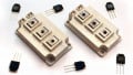
Figure 1: (a) SMA Package (b) SOD-123W package
Newer packages with flat leads and exposed solder pads transport the heat more efficiently and waste less space on a PCB. The same 50mil die from an SMA can also be manufactured in a SOD-123W package. The die / package footprint ratio is now > 20%. The heat is directly transferred out of the package. An added benefit is the height reduction of 2.5mm for the SMA to 1.02mm for the SOD-123W
So existing die and new die, currently used in SMA/B/C packages, can now be placed in smaller packages. A lot of combinations are possible, depending on the product and the application but in general, the SMC package can be replaced by the TO-277A/SMPC package, the SMB can be replaced by the SOD-128 and the Thin SMA, and the SMA by the SOD-123W, and the SOD-123HE.

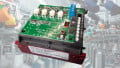
Figure 2: Smaller solutions by Taiwan Semiconductor for selected SMD-Packages
The transient thermal resistance and the thermal resistance/power dissipation in the application will determine if a size reduction is possible.
Absolute Maximum Ratings of Rectifiers
Tj= Ta+ Pd*Rthj-a is the most important equation when designing with rectifiers. The absolute maximum ratings of a rectifier are the Tj (junction temperature), the Ifsm surge current and the maximum breakdown voltage. The current rating and power dissipation (as well as current derating curves) are determined by marketing and designers who choose the size of the solder pads / PCB materials (Thermal Resistance). The Junction temperature is linked to the power dissipation (Pd) and the Thermal Resistance Rthj-a. So both package design and die technology contribute. The Ifsm surge current is mainly linked to the die size and the Zth. The breakdown voltage is determined by the die. In a TVs, the maximum peak power dissipation is linked to the die and the Zth.
Transient Thermal Impedance
The Transient Thermal Impedance of a Rectifier and a TVS diode is rarely discussed. Lightning strikes, 8/20us pulses or capacitive inrush surge currents (in AC/DC conversion designs) are single-pulse events, not repetitive. The product either survives or fails. The capability of a product to handle these surges is mainly dependent on the die size and the quality of the solder joint. For surges of 1ms or less, it is possible to reduce the package size without any degradation of the electrical performance if you keep the die size the same.
TVS diodes don’t really follow the Tj= Ta+ Pd*Rthj-a formula if we assume that the application is a single pulse event. They have a Peak Power Rating of eg 400W linked to a certain pulse – in most cases a 10/1000µs exponential waveform. The Tj max may be briefly exceeded during this test – the product has to survive the test without damage. Product capability is determined by the die size. The new packages introduced have a better die size to footprint ratio so product miniaturization is straightforward if you keep the die size the same.
The 1N4007 series or S1 series of standard rectifiers are some of the most common products used in low power AC/DC conversion. Billions of these rectifiers are manufactured every year. In an input bridge of a Flyback Converter < 20W, the power dissipation is quite small ( <100mA) . Their limiting factor is the IFSM surge rating. When the die from an S1 is placed in a smaller package, the IFSM rating may stay the same. For AC/DC applications, the S1 can be routed on both sides of the PCB. A surprising amount of rectifiers are routed on the bottom of the PCB, on the wave soldering side, and here the lower height is most beneficial
Thermal Resistance
The thermal resistance Rthj-a Junction to Ambient consists of 2 parts: a package related part and the contribution made by the solder pads – determined by the designer. In most designs on a single layer FR-4 PCB , the solder pads make by far the largest contribution to the total thermal resistance. This makes miniaturization difficult if a lot of power is dissipated. Very few designers use 5x5mm solder pad areas, typically used in datasheets to determine the thermal resistance. They tend to use the suggested solder pads for soldering, which are smaller (in some cases just 10-20% of the 5x5mm solder pads used to measure the thermal resistance) Expect an increase of 10 to 15K/W in Rthj-a

Figure 3: Part Average Testing
Two-layer and four-layer PCBs, thermal vias, and IMS substrates are options to make overall Rth less dependent on very large size solder pads. New rectifier packages with exposed pads can help in reducing board space in relation to the power dissipated. They also reduce the Tj by reducing Rthjl, improving reliability. Current ratings of especially Schottky diodes have been increasing in small packages. This does not mean that designers can use these packages at higher currents – but the power losses can be reduced by 10-20% due to the bigger die and the lower Vf. In the formula Tj = Ta + Pd * Rthj-a it becomes immediately clear that you cannot increase power dissipation without reducing thermal resistance (for a given package). Increasing the Tj would reduce your reliability. Trench Schottky technology is a major contributor to the package size reduction and increased efficiency.
Zero Defects
Rectifiers are mainly produced using GPP processes and in 4-inch fabs. Huge steps forward have been made in reliably producing rectifiers. TSC now manages a ppb level of less than 10ppb on its rectifier products. Rectifiers are older components. The 1N4007 was introduced in 1965. The S1 is more than 30 years old. A very important contribution to a zero-defects strategy is Part Average Testing (PAT). The test specifications on the main parameters are set to 4 or 6 sigma values by software. Especially on the leakage currents, datasheet values do not reflect the natural distribution. Even if Ir testing is reduced to 1µA instead of the 5µA datasheet value, a lot of products with potential mechanical damage, passivation problems and contamination issues can be shipped to customers. These products have reduced reliability and may produce early HTRB or Intermittent Op Life failures. PAT testing eliminates these.
In AC/DC conversion applications, no 100% OQC test is possible to monitor Ifsm – the surge rating – of a rectifier. A Delta Vf test (measuring the Vf before and after a short current pulse) monitors the thermal resistance and eliminates the worst soldered devices. When SMA devices were first introduced they were manufactured using belt furnaces for soldering. These processes had inherent issues with solder voids and fluctuations in Ifsm surge capability. New backend soldering improvements with matrix lines/vacuum soldering eliminate these risks. The SMD packages discussed are now manufactured using fully automated equipment in a cleanroom environment. This is also a major contributor to achieving zero defects.
About the Author
Jos van Loo is a technical expert for Power Semiconductors for more than 30 years. In his role as Technical Support Engineer at Taiwan Semiconductor Europe GmbH, Jos consults customers on Rectifiers, MOSFETs and Power Management ICs.