Facebook
 Google
 GitHub
 Linkedin
How to use a small microcontroller to control the LED driver for a dimmable triac
This article offers a method on using a small microcontroller to control the LED driver for a dimmable TRIAC for inherent power factor correction.
A microcontroller can be used to control an LED driver that is compatible with triac dimmers and only requires a small firmware overhead, giving users the capacity to add algorithms to improve the design, bring intelligence to the system or measure any of the parameters. This method is attractive because of its inherent power factor correction (PFC).
The design uses a high power factor flyback converter operating in critical conduction mode (CCM), which is the boundary between continuous and discontinuous inductor current mode. Basically, the topology is a conventional flyback except there is no bulk capacitor after the full-bridge rectifier. This means the rectified sinusoid can be used as the input of the converter rather than a fixed DC voltage.
This method uses Microchip’s PIC12HV752 eight-pin microcontroller with on-chip output waveform generator (COG) and the hardware limit timer (HLT) peripherals that are suitable for power conversion applications. The main purpose of the COG in this circuit is to convert two separate input events into a single PWM output. The HLT acts as a timed hardware limit to be used with asynchronous analogue feedback applications. The internal reset source synchronises the HLT with the analogue application.
Other peripherals include IO ports, a fixed voltage reference (FVR), comparators, a digital-to-analogue converter (DAC), timers, a capture-compare PWM (CCP) and an analogue-to-digital converter (ADC). This combination will produce a dimmable triac with active 0.95 PFC, 90 to 240V AC input and 20V DC, 325mA maximum output.
The comparators interface analogue circuits to a digital circuit by comparing two analogue voltages and providing a digital indication of their relative magnitude. The 5bit DAC module translates the rectified input voltage. The ADC converts the input signal into a 10bit binary representation.
Advantages
The incandescent lamp works well with a triac dimmer because it is purely resistive. Therefore, to design an LED driver compatible with a triac dimmer, the input characteristics of the LED driver should also be resistive. PFC can make the LED driver look like a pure resistor from the AC input side by making the input line current in-phase with the input line voltage.
Aside from the high PF, there are other advantages this topology can provide such as isolation between the AC mains and the converter output, which is desirable for safety requirements. It also reduces the need for heat sinks. CCM ensures low switching losses of the MOSFET. The high PF reduces dissipation in the bridge rectifier and the low part count helps reduce cost and form factor. A small size ,cheaper film capacitor replaces the bulky and costly high-voltage electrolytic capacitor after the full-bridge rectifier.
How it works
Figure 1 shows the simplified circuit of the LED driver with the PIC microcontroller controlling the circuit at the primary side, using the on-chip peripherals mentioned.

Figure 1: Simplified schematic of dimmable triac LED driver
The COG peripheral provides a PWM signal that drives the input of the MCP1416 MOSFET driver to turn on and off the MOSFET (Q1). The rising edge of the PWM is controlled by the HLT or the C1 comparator, while the falling edge is controlled by the C2 comparator. The input of C1 is derived from the voltage of the auxiliary winding of transformer T1, which is compared with VSS to detect the zero crossing of the auxiliary winding voltage (Vaux). The input of C2 is the voltage across the Rsense resistor, which is compared with the DAC output. The DAC output depends on its Vref, which is connected to the input wave shape signal, derived from the rectified input signal through a simple voltage divider.
The main advantage of primary side control is implementing PFC, achieved through the feed forward method and peak current mode control.
Start up
When applying the AC input voltage, the base voltage of transistor Q4 in the bootstrap circuit in Figure 2 is increasing. When there is enough base voltage, Q4 turns on and diode D14 is forward biased.

Figure 2: Bootstrap circuit
The voltage across the base of Q4 is held up to 10V by the D13 Zener diode. When Q4 turns on, the collector current flows through RC and D14 to increase the VDD of the PIC microcontroller. When VDD is high enough (usually the minimum VDD of the microcontroller) HLT, COG, DAC, ADC and comparators are initialised, after which the HLT emits a pulse at 58kHz to turn on Q1 initially. This will energise the primary inductance of T1 and transfer the magnetising current to produce Vaux when Q1 turns off.
Once the rectified Vaux has reached 10V, the forward voltage of D14 drops below 0.7V. This allows D14 not to conduct and Q4 to turn off. Once Q4 is off, VDD is supplied by Vaux. It is important that Q4 is always off during normal circuit operation to avoid power dissipation on Q4. Q4 remains off as long as there is enough Vaux. The operation of the bootstrap circuit is depicted through the waveform shown in Figure 3.
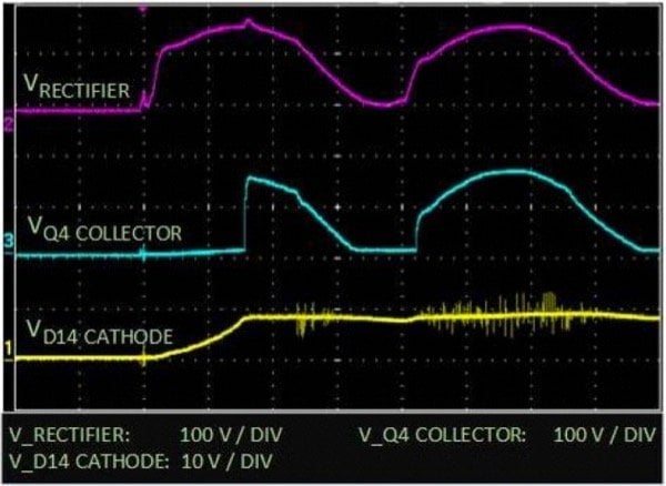
Figure 3: Bootstrap waveform
Steady state
When Q1 is on, the secondary diode D2 is off and the voltage across the T1 primary magnetising inductance (VLP) is equal to Vin(f), which is the rectified input voltage and is equal to the peak input voltage (Vpk) multiplied by the rectified input line phase angle. Also when Q1 is on, the primary inductance current (ILP) is increasing linearly. This current will flow through the Rsense resistor, the voltage drop across which is used as a sense voltage (Vsense) to translate ILP.
Due to the turn-on event of Q1, ILP is usually affected by a noise that is eventually reflected to Vsense, as shown in Figure 4. To prevent this switching noise from causing a false trigger, the COG peripheral uses the comparator blanking timers to count off a few cycles.

Figure 4: Switching noise on Vsense
Vsense is compared with the DAC voltage (VDAC) – which is also the peak current set point – by the C2 comparator. VDAC is derived from the rectified input voltage through a voltage divider so it follows the rectified input and forces the peak current of primary inductance (ILpk) to be synchronised and proportional to the rectified input. This is how the circuit achieves the PFC function. When Vsense reaches VDAC, Q1 turns off and HLT is reset.
As mentioned, the design is working in CCM. To ensure this conduction mode operation, Q1 should turn on again when ILS (secondary inductance current) reaches zero. This is made possible through zero current detection using C1, which detects ILS zero crossing based on Vaux. Figure 5 shows a timing diagram to visualise the control operation from start-up to steady state.

Figure 5: LED driver control timing diagram
Additional circuits
Figure 1 shows some circuit blocks that are included in the design to improve the reliability. The inrush current circuit is an active circuit that protects the primary side components by suppressing the large input current spikes. The bleeder circuit draws additional current to maintain the triac holding current at low input line voltage. Not maintaining the required holding current of the triac will cause it to misfire. The circuit is shown in Figure 6.
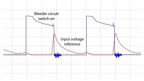
Figure 6: Switching of bleeder circuit
The snubber circuit is used to protect Q1 from a large voltage spike caused by the leakage inductance of T1. When Q1 turns off, the energy from the leakage inductance is reflected back to primary winding. The snubber circuit dissipates this energy to reduce the voltage spike.
Firmware
The firmware’s overhead is small and mainly consists of initialising the core independent peripherals. The pins on the PIC device are configured according to their function. After the pins have been configured, the peripherals are setup and turned on. During the initialisation, the internal connections and functions of the peripherals are established.
The ADC detects the status of the triac dimmer. If the rectified input voltage sampled by the ADC exceeds the triac minimum holding current threshold voltage, the bleeder circuit turns off, otherwise, it will turn on. Before the bleeder circuit turns on, a certain delay is required to evaluate the state of triac dimmer.
Conclusion
For a smooth dimming and a quiet operation, a challenge is to avoid unwanted triac switching caused by the ringing that occurs when the triac is initially fired. The input filter of this LED driver design requires an optimisation to avoid this problem and ensure that the line waveform will not be altered.
That said, the circuit presented here shows how a PIC microcontroller can control an LED driver that is compatible with traditional triac dimmers.
About the Authors
Kristine Angelica Sumague works as an Application Engineer at Microchip Technology Inc. - Philippines, where she has almost 6 years experience in the semiconductor industry focusing on firmware and hardware development from schematic design, hardware layout, testing and validation, and software development for applications like sensors and Switch-mode power supplies (SMPS). She earned her Bachelor's Degree in Electrical, Electronics and Communications Engineering at First Asia Institute of Technology and Humanities. She also holds a Master's Degree in Electrical, Electronics and Communications Engineering at De La Salle University located in the Philippines.
Mark Pallones works as the Principal Applications Engineer at Microchip Technology Inc. - Philippines, where he is responsible for managing teams to support new product development, introduction and development tools. He has authored and co-authored numerous applications notes, briefs, reference design and articles. He is particularly skilled in the field of circuit and PCB design and testing. He earned his Bachelor's Degree in Electronics and Communication Engineering at New Era University located in Quezon City, Manila, Philippines. He then proceeded for Post Graduate in Electrical Engineering Major in Power Electronics at the University of the Philippines. He then acquired his Master's Degree in Electronics Engineering at Ateneo de Manila University.