Facebook
 Google
 GitHub
 Linkedin
Highest Power density by 7th Gen IGBT StdType Module with New TMSTechnology
This article highlights Mitsubishi Electric 7th Gen. Std-type IGBT Modules based on TMS-Technology that is the 7th Gen Chip in the T-Series IGBT Modules.
The main requirements of power electronics systems are high efficiency, high power density and high reliability. To achieve the high efficiency Mitsubishi Electric developed the 7th Gen. IGBT chipset. To additionally fulfill the requirements of high power density and high reliability, the newly developed TMS package technology is combined with the 7th Gen Chip in the T-Series IGBT Modules in market de facto standard housings.
Industrial IGBT Modules are used in various fields of applications. All those applications require compact power modules with high power density, high reliability, low package inductance and high efficiency.
To fulfill all these requirements, the 7th Gen. Std-type IGBT Modules based on TMS-Technology have been developed. The 7th Gen. IGBT, which is based on CSTBTTM concept, provides high efficiency by reducing both dynamic and static losses. The loss reduction is the first step to realize a high power density module. In a second step the thermal resistance Rth must be improved in order to increase the power capability at a given operation temperature and to reduce the temperature swings. The newly developed TMS package technology provides very low thermal resistance, low package inductance and high thermal cycling capability.
TMS-Technology
The TMS (Thick Metal Substrate) Technology is a newly developed package technology for realizing low inductance and very high thermal conductivity. The comparison of the new TMS-Technology package structure with a conventional structure is shown in Figure 1.
In the conventional package structure the metalized ceramic substrates are soldered to a copper baseplate. By different CTE (Coefficient of Thermal Expansion) values of the copper baseplate and the ceramic substrates this solder layer is stressed by temperature cycles which are limiting the module life time.
Due to this mechanical stress applied to the solder layer, the maximum substrates size is limited. Therefore by using the conventional structure several substrates have to be used in order to realize IGBT Module with e.g. 62 x 108mm² baseplate size. The needed wire bond connections in between those substrates are resulting in higher package inductance, higher lead resistance and less usable area for the power chips.
The low specific thermal conductivity of the solder material is increasing the thermal resistance. For minimizing these disadvantages of high thermal resistance, limited reliability of substrate solder, package stray inductance, lead resistance and less effective area, the new TMS-Technology is developed and introduced to 7th gen. Std-type IGBT Module.
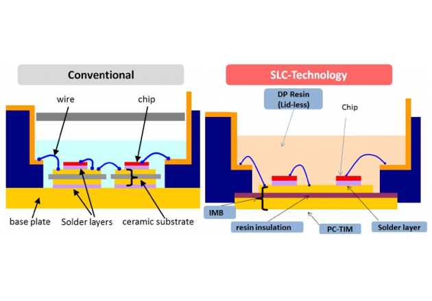
Figure 1: Comparison of Conventional Module and TMS-Technology package structures
TMS replaces the conventional package structure
The TMS replaces the conventional package structure with baseplate and several ceramic substrates. This TMS contains at top and bottom side thick copper layers which are brazed to a high thermal conductive silicon nitride (Si3N4) ceramic [4]. The thick copper layer on the topside provides a low electrical resistance, which reduces the losses or allows increasing the current density of the conductors. A second advantage is an improved heat spreading directly under the chips.
In combination with the elimination of substrate solder layer the Rth(j-c) is essentially improved. In conventional modules with copper baseplate and ceramics substrate, a warping of the baseplate also has to be considered during temperature cycles due to the unmatched CTEs and the resulting “bi-metal effect” [3]. This warping limits the possibility to improve the thermal resistance between baseplate and heat sink Rth(c-s). With the new TMS-technology which has and an symmetric sandwich construction, this warping can be reduced and the thermal interface between baseplate and heat sink can be further improved by using an optimized pre-applied phase change thermal interface material (PC-TIM). The total thermal resistance from junction to heat sink
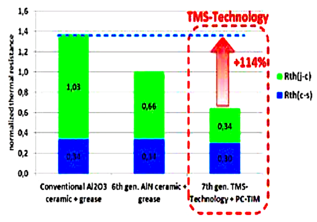
Figure 2: Rth comparison of TMS-Technology and Conventional Module and package structures at same chip size
of a conventional module with widely used aluminum oxide ceramic is about 114% higher than TMS-technology at same chip sizes as shown in Figure 2. Also the previous 6th gen. IGBTs Modules, which are based on high thermal conductive aluminum nitride ceramic, has an about 56% higher thermal resistance compared to the new TMS Technology.
The thermal cycling test result, as shown in Figure 3, shows that the brazing of the copper layers to the Si3N4 ceramic is a reliable connection. After 1000 temperature cycles from -40°C to 125°C no delamination could be observed in TMS whereas in the conventional package structure after 300 cycles first solder cracks in the corner of the substrate are already visible.
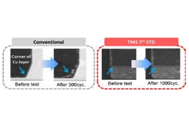
Figure 3: Thermal cycle test result for Tc cycle of -40°C to 125°C
7th Gen Std-type IGBT Modules
The new TMS-technology together with the 7th Gen IGBT chipset is introduced in the Std-type Modules Series of Mitsubishi Electric.
The 7th Gen IGBT chip has an improved trade-off of collector emitter saturation voltage Vce(sat) vs. turn-OFF switching energy Eoff. The cell design is optimized to have an improved controllability of the dv/ dt by the gate resistor. By using of RFC structure (Relaxed Field of Cathode) for the freewheeling diode it is possible to improve also the trade-off of recovery losses and forward voltage drop by keeping the soft recovery behavior [2].
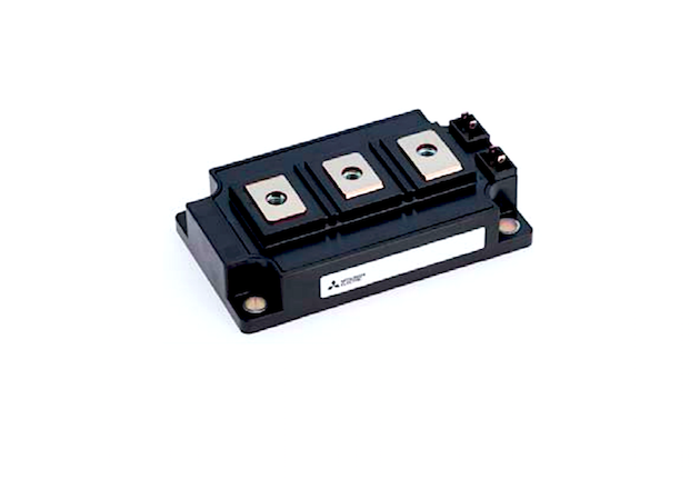
Figure 4: 7th gen Std-type 62mm 2in1 IGBT Module
The characteristics of the new chip set was evaluated and used for the simulation of losses with the Mitsubishi simulation software called MELCOSIM [1]. The result is that e.g. the 1200V class 7th Gen IGBT can save about 15% of total losses compared to the 6th Gen IGBT under typical motor control inverter application conditions.
To support the inverter assembly process on customer side, all 7th Gen. Std-type Modules will be optional available with the optimized PC-TIM. Figure 5 shows that this Std-type 7th Gen IGBT Modules with TMS technology is under development with a comprehensive line-up to support wide range of applications with these new technologies.
Highest power density
The superior thermal performance of the TMS-technology in combination with the low loss 7th gen. chipset provides the possibility to reach a new level in terms of power density for IGBT Modules.
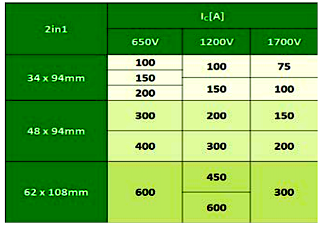
Figure 5: Line-up plan of 7th gen Std-type IGBT Modules
Package outline of the 62mm Std-type packag
The package outline of the 62mm Std-type package is a de facto standard and available from several different power module suppliers. Depending on the rated current definition the maximum available current rating in the market is 300A up to 450A for 1200V class IGBT Modules. With the 7th gen Std-type Module a current rating of 600A is realized in the 62mm package.
This new level of current density is shown in Figure 6 and compared with the other available 62mm type Modules from the market. In this comparison the maximum output current is calculated for various switching frequencies. The condition are typical inverter operation conditions with minimum gate resistance specified in each datasheet and a fixed temperature rise from junction to case of ∆T(j-c)=15K is considered.
The result is that by changing from market standard available 62mm Module with 300~450A to the new CM600DY-24T the output current and power can be increased by about 130% for a switching frequency of 4kHz. Or by keeping the output current the switching frequency could be increased by a factor of about seven.
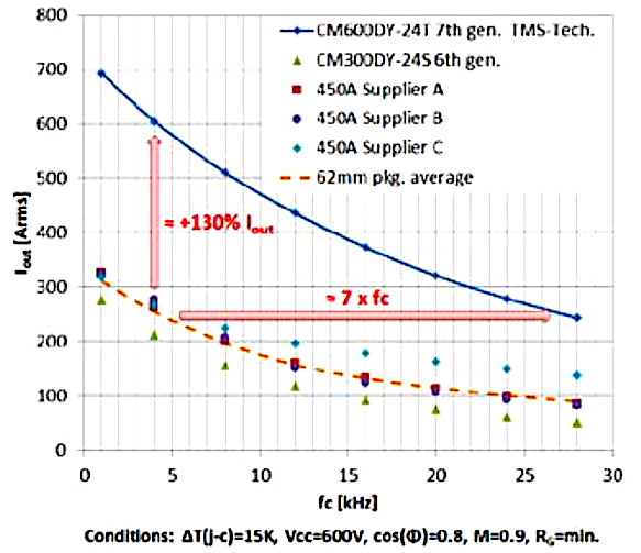
Figure 6: Output current vs. switching frequency for different 62mm 1200V 2in1 IGBT Modules
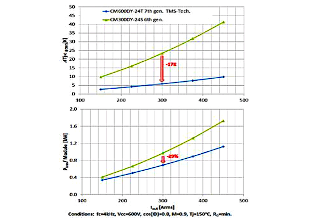
Figure 7: Losses and ∆T(j-c) vs. output current of maximum current rating 62mm Modules of 6th and 7th gen. IGBT
In a different way, the inverter efficiency can be improved by changing from existing 62mm Module to new 600A 7th Gen IGBT Module as shown in Figure 7. Especially the applications in the field of renewable energy or UPS have requirement for high efficiency and could utilize the advanced characteristics of the 600A Module. For example, for an output current of 300Arms the losses can be reduced by about 29%.
Other applications like servo inverters or elevators usually have to consider lifetime limitations by power and thermal cycling. If we compare the related temperature rise ∆T(j-c) in Figure 7 we see that at 300Arms output current it is decreased by about 17K. If we consider the strong dependency of power cycling capability on the temperature swings this 17K reduction could increase the inverter lifetime by a factor of 10 to 20 depending on the actual used wire bond technology.
Summary
A series of Mitsubishi IGBT modules for 650V, 1200V and 1700V rated voltage has been developed covering a wide current range based on the well-established Std.-package style. The IGBT module series combines the latest 7th generation IGBT- and FWDi-chips with an innovative packaging technology, called TMS-technology. The new IGBT module series is enabling inverter designs with higher output currents, higher power density and improved reliability.
The level of power density is demonstrated with the 600A/1200V IGBT Module in the 62mm package. By changing from existing 300~450A/1200V 62mm Module to the 7th gen 600A the following improvements options could be achieved:
- Increase inverter output power by about 130%
- Increase inverter switching frequency by factor 7
- Power loss reduction by about 29%
- Increased power cycle life time by reduced temperature swing
About the Authors
Thomas Radke worked as an assistant manager business development power semiconductor at Mitsubishi Electric Europe - German. Mitsubishi Electric operates on the corporate principle of contributing to creating a vibrant and affluent society by enhancing its technologies, services, and creative powers, as a leader in the manufacture and sales of electric and electronic equipment used in Energy and Electric Systems, Industrial Automation, Information and Communication Systems, Electronic Devices, and Home Appliances.
Satoshi Miyahara received his Master of Engineering in the Field of Hydrogen Energy System at Kyushu University Graduate School. He worked as an application engineer at Mitsubishi Electric, in which this company is leader in the manufacture and sales of electric and electronic equipment used in Energy and Electric Systems, Industrial Automation, Information and Communication Systems, Electronic Devices, and Home Appliances.
References
- MELCOSIM: IGBT thermal and loss simulation software, available at www.mitsubishielectric.com/semiconductors/simulator/
- T. Radke; K. Masuda: “7th Gen. IGBT and Diode Chip-set Enabling Highest Performance Power Modules”, Bodo’s Power Systems June 2015, page 42-35
- T. Radke; K. Masuda: “More Power and Higher Reliability by 7th Gen. IGBT Module with New SLC-Technology”, Bodo’s Power Systems August 2015, page 24-26
- M. Miyazawa, et al: “7th Generation Module for Industrial Applications”, PCIM Europe 2014, page 34-38, ISBN 978-3-8007-3603-4