Facebook
 Google
 GitHub
 Linkedin
High Voltage Power Semiconductor Modules with Enhanced Insulation Properties
This article features JSC Proton-Electrotex research and development to find structural and technological solutions providing increased insulation strength.
One of the main parameters related to reliability and safety of power semiconductor modules is the strength of electric insulation. Breakdown of the electric insulation not only causes failure of the module, but also damages the entire converter leading to high financial losses. This article discusses the current situation on the market of bipolar power modules, the importance of improving their insulation properties and stability of insulating properties throughout the entire life cycle. The Proton-Electrotex company has carried out research and development to find structural and technological solutions providing increased insulation strength up to 7 kV (AC) throughout the entire service life.
The current market situation and relevance of the problem
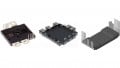
Power semiconductor devices are one of the primary elements of electrical energy converters. The power electronics market features devices for various power ranges in disc, stud and module versions. Each of these designs has its own advantages and disadvantages. The widespread use of power semiconductor modules with insulated basement results from their easy mounting, optimal weight and dimensions.
Power modules with a base width of 60 mm (A2-type modules by the Proton-Electrotex designation) found wide application in the market. Modern serial modules with this design normally have insulation voltage of 3-3.6 kV (AC, 50 Hz, 60 seconds).
However, modules with higher insulation voltages up to 7 kV (AC, 50 Hz, 60 seconds) become more demanded on the market too. Module designs currently offered on the market usually do not meet such requirements.
The main reasons of their limited electric strength value are:
- Breakdown of insulation to the base, either due to insufficient width of the ceramic insulator, or presence of irregularities of the insulating gel (foreign inclusions or air bubbles), or unsuitable structure of the area responsible for isolating the base from elements with a potential.
- Overlap between module elements having different potentials, either due to the presence of irregularities of the insulating gel (foreign inclusions or air bubbles), or due to the penetration of moisture, conductive dust or other ionic materials.
It is worth to note the importance of not only the high dielectric strength of the power module, but also its stability throughout the entire period of operation. The process of insulating properties degradation is inevitable during operation of the module.
There are several factors affecting the rate of insulation strength degradation, including:
- factors related to design and manufacturing technologies;
- factors related to microclimate of the operating environment.
The first group of factors includes changes in polymerization chains of the insulating gel during operation due to thermal processes, and influence of partial discharges in the insulating elements.
The second group of factors includes presence of moisture and / or conductive dust in the power module.
One of the most important aspects affecting degradation of the electrical insulation strength is the occurrence of partial discharges.
Research subject. Approach to testing
A research program based on potential-free MD3-320-65-A2-type power modules was carried out to find design and manufacturing solutions ensuring increased insulation strength up to 7 kV (AC) throughout the entire module service life.
A complicated test procedure was used to measure the electrical strength of modules with the new solutions, including the following successive stages:
- test for insulation strength at room temperature at 7 kV (AC, 50 Hz, 60 seconds);
- test for effects of static dust according to standard GOST 20.57.406 (the dust was not removed after the tests);
- tests for resistance to high humidity, GOST 20.57.406;
- treatment of the modules with saline solution;
- measurement of insulation strength.
As such, the tests were held in more demanding conditions than the normal operating environment required by the climatic version according to GOST 15150, ensuring reliability of the devices in actual operating conditions.
It was established that the suggested measures not only increased the insulation strength of a semiconductor module, but also effectively protected it from surface discharges bypassing though the conductive dust.
Stability of the module insulation properties over time
Stability of the module insulation properties over time becomes especially important as the range of blocking voltage grows wider. One of such properties is the amount of partial discharges. Partial discharge (PD) is a type of spark discharge of very low power occurring inside insulating materials in equipment of medium and high voltage classes [2].
A review of publications confirms the relevance of the problem of partial discharges in insulation of high-voltage equipment, but there are very few references related to bipolar semiconductor devices. Typically, isolation gets damaged by PD over many months or even years. In most cases, analysis of the reasons for such failures is not carried out and the topic remains without proper attention.
In other words, the lower the insulation voltage, the longer the defect does not manifest itself, and if the insulation voltage is below 3000 V, PD does not occur at all. The amount of power bipolar modules with a blocking voltage above 3.6 kV on the market is low, while the amount of failures due to other reasons is quite large, so failures associated with insulation degradation due to the occurrence of a PD are not predominant.
However, the situation is different for power modules with blocking voltage up to 6.5 kV, since the time before the critical degradation of the insulating properties due to PD is dramatically reduced. Therefore, when designing and manufacturing power modules with insulation voltages up to 7 kV, it is extremely important to monitor the characteristics of the partial discharge.
Currently there are many available methods to measure PD parameters, including:
- electric;
- electromagnetic, or remote, microwave method;
- acoustic;
- chemical;
- optical or optoelectronic;
- thermal [1].
Proton-Electrotex is currently engaged in studies of PD properties in power modules with a base width of 60 mm and insulation voltage of up to 7 kV and identifying the mechanisms of their formation.
The workstation required to measure PD consists of:
- Measuring system Omicron MPD 600.
- High-voltage transformer.
- A coupling capacitor with minimal inductance.
- Calibrator Omicron CAL 542 1 - 100 pC.
- Sensor of partial discharge current.
- Systems to process the measurement results.

Figure 1: Functional diagram of the measurement system, where:U – high voltage power supply; Zmi – input impedance of the measuring system; CC – connecting cable; Ca – test object; Ck – coupling capacitor; CD – coupling device; MI – measuring device; Z – filter.
To reduce the level of interference caused by external electric fields, the entire measuring system is placed in a Faraday cage. Measurements of all samples are made according to an electrical method meeting GOST R 55191 (IEC 60270: 2000). Functional diagram of the system is shown in Figure 1 [3].
Software used to process the measurement results offers additional features:
- visual rendering (Figure 2) of the PD in real time with reference to the phase of the test input;
- measurement of the charge over time;
- counting the amount PDs exceeding a given level of intensity;
- generation of an integral picture of PD for the entire testing duration. The integral picture allows to identify not only the partial discharge, but also surface leakage, corona discharges, etc.

Figure 2: Visualization of the PD measurement results for a device with a critical level of PD
The measurement process can be described as follows:
1. Before testing, each sample was measured for insulation resistance at 5 kV (AC, 60 seconds).
2. Test voltage of 3580 V (AC) was applied to the tested sample and maintained for 5 s, then decreased to 2860 V (AC) and maintained for 30 s [4]. Measurements of PD characteristics were performed at the end of the second time interval (Figure 3).
3. All results for each sample were recorded in the test report.

Figure 3: Mode of measuring PD characteristics
Each sample was measured for the following:
- quantitative amount of the partial discharge – the value of the “apparent charge” in pC at 2860 V;
- the voltage value when a partial discharge does not occur;
- the voltage value when a partial discharge occurs.
This measurement method complies with GOST R IEC 60664.1-2012 standard “Insulation coordination for equipment in low-voltage systems” Part 1.
Research results and conclusions
Solving the problem associated with PD in power semiconductor modules is complicated by a number of factors related to their design. One of these factors is presence of several interpotential zones inside the device, where partial discharge can occur. This greatly complicates localizing defects in the initial stages of the study. The task is also complicated by various types of insulation materials with different properties inside the module.
The Proton-Electrotex company was able to localize the zones where partial discharges occur using differentiated analysis of the structure, allowing to take measures to reduce their intensity (Figure 4). Combined with actions to increase the insulation strength up to 7 kV, such measures can improve the safety and reliability of high-voltage devices with an insulation voltage of up to 7 kV (AC) throughout their entire service life.

Figure 4: Visualization of the PD measurement results for a device without PD
References
- Andreev, A. M. «Metody ispytanij dielektrikov. Izmerenie harak-teristik chastichnyh razryadov v elektricheskoj izolyacii uchebnoe posobie dlya studentov vysshih uchebnyh zavedenij, obuchayush-chihsya po napravleniyu podgotovki magistrov „Tekhnicheskaya fizika“». Polytechnic University Publishing House.
- Rusov, V.A., Izmerenie chastichnyh razryadov v izolyacii vysokovol’tnogo oborudovaniya. — Ekaterinburg, USURT, 2011.
- GOST R 55191-2012 (MEK 60270:2000) Metody ispytanij vyso-kim napryazheniem. Izmereniya chastichnyh razryadov. – Moscow: Standartinform, 2014
- GOST R MEK 60664.1-2012 Koordinaciya izolyacii dlya oborudo-vaniya v nizkovol’tnyh sistemah. CHast’ 1. Principy, trebovaniya i ispytaniya – Moscow: Standartinform, 2014
About Proton-Electrotex
Proton-Electrotex is one of the Russian leaders in the design and manufacture of power semiconductor diodes, thyristors, modules, coolers, IGBTs (IGBTs), as well as power units for use in various electric energy converters. The company was founded and began production in 1996 on the leased premises of the Proton plant. Since then, Proton-Electrotex has developed its own infrastructure for the entire production cycle. Production is equipped with modern production lines, measuring equipment of our own production and areas for “clean technologies” with full compliance with the requirements for electronic products and microelectronics.
This article originally appeared in the Bodo’s Power Systems magazine.