Facebook
 Google
 GitHub
 Linkedin
Gaining Speed: Mitsubishi Electric SiC-Power Modules
The article focuses on high-voltage SiC-modules and gives insights to features and applications.
Back in September 2017, we published an overview in Bodo's Power about the history and status of our SiC-power modules covering a wide range of commercially available SiC-modules from several ten amps up to 1200 A and rated voltages from 600V to 3300V [1]. Today, one year later, the SiC technology has gained further speed. The present article is giving a survey about Mitsubishi Electric’s latest achievements on SiC power modules with regard to research, product development, and applications. The main focus of this article is high-voltage SiC-modules.
SiC Research in Japan
The research activities on SiC are coordinated in Japan by an organization called NEDO (New Energy and Industrial Development Organization). NEDO is Japan’s largest public R&D management organization for coordinating the innovation efforts in strategic directions. The development of high power density and high withstand voltage SiC power modules is one of NEDO’s main R&D directions and Mitsubishi Electric is a key player in this activity [2]. Several outstanding Mitsubishi Electric R&D results on SiC technology reported in this article have been supported by NEDO.
Embedding Schottky-Barrier-Diodes into SiC-MOSFETs
The design for embedding Schottky-barrier-diodes (SBD) directly into MOSFET chips is shown in Figure 1 [3].

Figure 1. Cross section of (a) a conventional SiC-MOSFET with external SBD and (b) an SBD-embedded SiC-MOSFET
As body diode operation may cause bipolar degradation by expansion of stacking faults in the SiC-MOSFET it is recommended to be avoided. Both cross-sectional structures shown in Figure 1 are achieving this objective by the same principle: As long as the forward voltage of SBD is lower than the built-in potential Vpn of the MOSFET’s body diode there will be no current flowing through the bipolar body diode.
Many SiC-modules available today [1] are using the approach (a). The research results reported in [3] show that by integrating the SBD into the MOSFET-chip (b) the condition “no bipolar body diode current flow” is achievable for remarkably higher SBD current densities than in the conventional structure (a) with external antiparallel SBD. Consequently, the active chip area needed for forming a functional switch (MOSFET + antiparallel diode) can be drastically reduced by using the approach (b).
In [4] the impact of embedding the Schottky-Barrier Diode into the SiC-MOSFET-chip is investigated for 3.3kV and 6.5kV SiC-MOSFETs. The reduction rate of active chip area is 50% for 3.3kV SiC-modules and 75% (!) for 6.5kV-modules, see Figure 2. This example is showing that the approach (b) is attractive especially for very high voltage SiC-MOSFETs.

Figure 2. Active area of 3.3kV and 6.5kV conventional SiC-MOSFET with external SBD compared with SBD-embedded SiC-MOSFET
On the other hand, the impact of integrating the SBD into the MOSFET on increasing (worsening) the specific on-resistance is small as shown Figure 3.

Figure 3. Specific on-resistances separated into channel resistance (red), drift resistance (green) and spread resistance (blue) in the 3.3kV and 6.5kV SBD-embedded SiC-MOSFETs at Tj=150°C compared to those in conventional SiC-MOSFETs [4]
The forward characteristics of new SBDembedded SiC-MOSFET samples are shown in Figure 4.

Figure 4. Drain characteristics of the 3.3kV and 6.5kV samples at room temperature and Tj=150°C [4]
New 6.5kV Full-SiC Dual Module
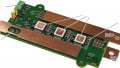
Based on the new 6.5kV SiC-MOSFETs with embedded SBD the Mitsubishi Electric Advanced Technology R&D Center announced in January 2018 [5] the world’s highest power density Full-SiC-Module representing 9.3kVA/cm³, see Figure 5. When comparing this power density with 5.1kVA/cm³ offered by best in class conventional 6.5kV Si-Power module the big potential for system size reduction becomes evident.

Figure 5. Prototype of 6.5kV Full-SiC Power Semiconductor Module
The performance of the new 6.5kV Full-SiC dual module is investigated in [6] under different aspects. Based on the recently developed new HV100 standard dual package [7], the internal module structure was optimized by 3D electromagnetic simulation for reducing the internal package inductance, for achieving a good dynamic current sharing among the paralleled SiC-MOSFET chips and for improving the EMI-robustness. Special attention was paid to eliminate the magnetic interference toward the gate caused by the high speed switching. The simulated turn-on waveforms before and after optimization are shown in Figure 6.

Figure 6. Simulated turn-on waveforms before and after optimization
The measured turn-on waveform at room temperature and Tj=175°C in Figure 7 show that switching speed at P- an N-side are almost the same. Furthermore, no significant differences in switching performance can be seen between room temperature and Tj=175°, indicating that the device performance is unipolar.

Figure 7. Comparison of turn-on waveforms of P- and N-side at (left) room temperature and (right) Tj=175°C
The total switching energy of new SBD-embedded 6.5kV Full-SiCMOSFET Module is less than 10% compared to conventional 6.5kV Si-IGBT Modules, see Figure 8.

Figure 8. Comparison of switching loss between Si-IGBT at Tj150°C, SiC MOSFET and SBD-embedded SiC MOSFET at 175°C
This drastic switching loss reduction is opening the door to high voltage power module applications with switching frequencies in the range of several kHz, where the today’s 6.5kV Si-HVIGBT-modules were found to be not really applicable, even when used in resonant mode (for example in solid-state transformer applications). As a reference, the power loss simulation shown in Figure 9 at 500Hz, 2kHz, and 10kHz is provided in [6].

Figure 9. Comparing power loss between Si-IGBT at Tj150°C, SiCMOSFET and SBD-embedded SiC-MOSFET at Tj=175°C
Improving the Short Circuit Capability of SiC-MOSFETs
One of the issues with today’s SiC-MOSFETs is their limited short circuit endurance. One way to increase the allowable short circuit time tsc would be to increase the on-resistance of the SiC-MOSFET. But this approach would lead to large on-state energy loss. The principle trade-off relationship between on-resistance and short circuit time tsc is explained in Figure 10.

Figure 10. Trade-off between on-resistance and short circuit time tsc
In [8] and [9] Mitsubishi Electric announced a new proprietary chip structure that is currently in R&D status to tackle this issue: by introducing an additional region into the source area, see Figure 11. By this means, the source series resistance of the SiC-MOSFET is controlled and the incidence of excessive current flow during short-circuit operation is reduced.

Figure 11. Cross-sectional view of the newly developed SiC-MOSFET
By this approach, a short circuit time tsc=8μs (similar to today’s Si- IGBT) is achievable without increasing the on-resistance significantly. According to Mitsubishi Electric’s press release dated September 2017 this new SiC-device is offering the world’s highest power efficiency rating of any 1200V-class power devices with a short–circuit time exceeding 8μs [9]. In Figure 12 the on-state resistance versus short-circuit time of new SiC-MOSFET is compared with conventional SiC-MOSFET. At tsc=8μs the specific on-resistance has been reduced by 40% compared to conventional SiC-MOSFET.

Figure 12. Specific on-resistance at room temperature versus shortcircuit time
Simulation of SiC-MOSFET Switching Behavior
Accurate simulation of transient switching behavior, for example of the drain-source voltage slope dvDS/dt and the drain current slope diD/ dt is important for optimizing the internal structure of SiC-MOSFET modules In [10] a new behavioral SiC-MOSFET model is described taking into account the internal stray inductances and capacitances. By using this model, it was possible to reproduce accurately the operation of paralleled SiC-MOSFETs even under thermally imbalanced conditions [11]. In [12] this model is further refined. The waveforms shown in Figure 13 indicate a good matching of simulated and experimental results. The new SiC-MOSFET model is a powerful tool for the simulation-based design of power electronic circuits [12].

Figure 13. Comparison of simulated and experimental waveforms of a 15A/1200V SiC-MOSFET during (a) turn-on and (b) turn-off
New 750A/3300V Full SiC Dual Module
The Mitsubishi Electric 750A/3300V Full-SiC Dual Module was announced at PCIM-Europe 2017 Conference [13]. Meanwhile, this device is commercially available; the type name is FMF750DC-66A. For minimizing the internal package inductances and for good current balancing among the paralleled chips the most advanced dual package for this voltage and power class, the new LV100 package, has been employed, see Figure 14.

Figure 14. FMF750DC-66A package outline
The two main options for system performance improvements with FMF750DC-66A versus conventional HVIGBT-modules are [14]:
-
Increasing the switching frequency by keeping the same (for the same cooling system) power loss level as with today’s Si-IGBTs. This direction is interesting for obtaining system benefits that were not reachable with today’s Si-HVIGBT-Modules due to their higher switching energy Esw. The simulation results reported in [14] are indicating that a same inverter output current level the switching frequency can be increased by a factor of 5…7 when using the FMF750DC-66A instead of its Si-HVIGBT counterpart.
-
Reducing the power loss (increasing the system efficiency) for reducing the cooling efforts by maintaining the switching frequency at similar level as with today’s HVIGBTs with the objective of:
-
Increasing the system’s power density (reducing the system size & weight);
-
Increasing the system efficiency for increasing the operation time of autonomous, battery-driven systems or for reducing the TCO caused by energy loss in permanently operating power conversion systems (for ex. UPS or PV-inverters).
-
Depending on the application requirements, also a mixture of both potential performance improvement options is possible.
When designing a power electronic system with Full-SiC Modules the question arises how to handle their higher switching speed compared with Si-IGBTs, especially their higher dvDS/dt. In [15] the influences of temperature, gate resistance and gate voltage on the switching performance of new FMF750DC-66A have been studied. In Figure 15, the turn-off waveforms for different gate resistors are given. Figure 16 shows the dependency of dvDS/dt on gate condition. The measured trade-off curves Eoff vs. dvDS/dt are shown in Figure 17.

Figure 15. Voltage transients during turn-off for different gate resistances (VDD=1800V, ID=750A, Tj=25°C, RG(off) = 0.9…6.2Ω)

Figure 16. Voltage slope during turn-on and turn-off for different gate resistances RG and gate voltages VGS

Figure 17. Turn off losses of FMF750DC-66A in dependency on dvDS/dt
In conclusion, the experimental investigations in [15] confirmed a good controllability of FMF750DC-66A voltage transients by the gate drive conditions.
Application Examples of High-Power SiC Modules in Japan
During the last International Power Electronics Conference (IPEC '18, held in Niigata, Japan in May 2018) several examples of applications using the Mitsubishi Electric SiC-Power Modules were shown:
- Using 1200A/1700V hybrid SiC-modules in a 600VDC tramcar showed a traction converter size reduced by 40% compared to a Si-IGBT system.
- Using 3300V full SiC-modules in a modular multilevel converter for HVDC-transmission showed a loss reduction of 50%, a size reduction by 21%, and a weight reduction by 14% compared to the solution with conventional Si-HVIGBT modules.
- Using SiC modules rather than IGBT modules in a 750kW PV-inverter reported a maximum efficiency of 99% [18], which is about 0.4% better than with conventional Si IGBTs.
Embedding Antiparallel Schottky-Diodes into SiC MOSFETS Reduces Chip Size
During the past year, Mitsubishi Electric has reported several outstanding achievements in high voltage SiC technology. A new 750A/3300V full SiC dual Module FMF750DC-66A was made commercially available. By embedding the antiparallel Schottky-Diode directly into the SiC-MOSFET chip it was possible to reduce the active chip area needed for 6.5kV-full SiC modules by 75% (!). By using this new SBD-embedded MOSFET chips a 6.5kV full SiC module was presented with the world’s highest power density of 9.3kVA/ cm³. Outstanding application benefits when using 1700V and 3300V SiC-Modules have been reported from several end-users in Japan indicating that the introduction of SiC-technology is gaining speed, particularly for high voltage applications. By the reported over the past year innovations, Mitsubishi Electric has proven its technology leadership for HV-SiC-modules.
About the Author
Junji Yamada (山田 順治) joined Mitsubishi Electric Corporation in 1985. After working for 5 years as an analog electronic circuit designer for engine ignition systems, he has been involved in power module development since 1990. He has been engaged in power module development for about 20 years, from bipolar systems such as transistor modules and diode modules to MOS systems such as MOSFET modules and IGBT modules. For three years from 2011, he belonged to the technical support department of the power module at the German branch, and returned to Japan in 2014. After returning to Japan, he belonged to the Applied Technology Department and was in charge of technical marketing, development planning, and sales expansion technical support. Now he works as the General Manager of the Applied Technology Department, Power Device Works at Mitsubishi Electric Corporation, Fukuoka, Japan.
Eckhard Thal graduated from the Moscow Power Engineering Institute in 1980. Same year he joined ELPRO Berlin as a design engineer in the inverter development. In 1991 he received his Ph.D. in the field of power electronics at the Chemnitz University. Since 1991 he is working for Mitsubishi Electric Europe (Ratingen/Germany) in application engineering for power semiconductors.
References
- J. Yamada, E. Thal, “SiC Power Modules for a Wide Application Range”, Bodo’s Power Systems, Sept. 2017, p.20-27
- S. Nomura, “NEDO’s Next-Generation Power Electronics Projects and Recent Activities”, IPEC’18, May 20-24, 2018, Niigata, Japan, Industrial Seminar, p.65-68
- K. Kawahara et al., “6.5kV Schottky-Barrier-Diode-Embedded SiC-MOSFET for compact Full-Unipolar Module”; ISPSD’17, May28-June1, 2017, Sapporo, Japan
- K. Kawahara et al., “Impact of Embedding Schottky Barrier Diodes into 3.3kV and 6.5kV SiC MOSFETs”; ICSCRM’17, September 17-22, 2017 Washington, D.C
- Mitsubishi Electric Press Release No.3164: “Mitsubishi Electric’s New 6.5kV Full-SiC Power Semiconductor Module Achieves World’s Highest Power Density”; Tokyo, January 31, 2018
- J. Nakashima et al., “6.5kV Full SiC Power Module (HV100) with SBD embedded SiC MOSFETs”; PCIM-Europe 2018, conference proceedings pp.441-447
- Mitsubishi Electric Press Release No.3018: “Mitsubishi Electric Develops HVIGBT Module X-Series New Dual”, Tokyo, April 6, 2016
- H. Hatta, “Advances in SiC power devices for power electronics applications”; IPEC’18, May 20.24, 2018 Niigata, Japan, Industrial Seminar, pp.58-64
- Mitsubishi Electric Press Release No.3129: “Mitsubishi Electric Develops SiC Power Device with Record Power Efficiency”, Tokyo, September 22, 2017
- Y. Mukunoki et al., “Modeling of a Silicon-Carbide MOSFET With Focus on Internal Stray Capacitances and Inductances, and Its Verification” IEEE Transactions on Industry Applications, Vol.54, No.3, May/June 2018, pp.2588-2597
- Y. Mukunoki et al., „Electro-Thermal Co-Simulation of two Parallel Connected SiC-MOSFETs under Thermally-Imbalanced Conditions”
- Y. Mukunoki et al., “An Improved Compact Model for a Silicon- Carbide MOSFET, and its Application to Accurate Circuit Simulation”, article accepted for publication in IEEE Transactions on Industry Applications, DOI 10.1109/TPEL.2018.2796583
- T. Negishi et al., “3.3kV All-SiC Power Module for Traction Use”, PCIM-Europe 2017, Conference Proceedings, pp.51-56
- N. Soltau et al., “3.3kV Full SiC MOSFETs – Towards High-Performance Traction Inverters”, Bodo’s Power Systems, January 2018, pp. 22-24
- N. Soltau et al., “Impact of Gate Control on the Switching Performance of a 750A/3300A Dual SiC Module”, paper at EPE2018 conference, September 17-21, 2018, Riga, Latvia
- S. Makishima et al., “The direct benefit of SiC Power Semiconductor Devices for Railway Vehicle Traction Inverters”, IPEC’18, May 20-24, 2018, Niigata, Japan, Conference proceedings, pp. 2047-2050
- Y. Ishii et al., “Verification of SiC-based Modular Multilevel Cascade Converter (MMCC) for HVDC Transmission Systems”, IPEC’18, May 20-24, 2018, Niigata, Japan, Conference proceedings, pp. 1834-1839
- M.Kinoshita, “Power Electronics Technology Contributing to Realizing a Sustainable Society”, IPEC’18, May 20.24, 2018 Niigata, Japan, Industrial Seminar, pp.53-57
This article originally appeared in the Bodo’s Power Systems magazine.