Facebook
 Google
 GitHub
 Linkedin
Field Failures in Power Modules—Potential Root Causes and How to Avoid Them
This article describes key factors in selecting and setting up power modules amid key factors such as harsh environments, field conditions, ventilation, and design.
This article is published by EEPower as part of an exclusive digital content partnership with Bodo’s Power Systems.
A variety of stressors act on the power module and the system, which need to be considered when selecting the modules and the respective materials. System manufacturers who integrate power modules in a final product (e.g., integrated power supply solutions) can actively influence the robustness of their systems here by selecting the power module suitable for their mission profile (performance versus costs) as well as through system design. Regarding system design, system manufacturers need to ensure that stress factors are minimized and not, in the worst case, amplified. For this, process deficiencies (e.g., during power module system integration), material and component selection, housing, and ventilation situation need to be discussed.
In addition to discussing the possible approaches to system design for improving system reliability, Zestron has gained experience over the past years with the application of rapid HAST (highly accelerated stress test) quality testing regarding module selection. These tests allow for an initial pre-selection of suitable modules before conducting the required but time-consuming qualification tests. Thus, they can reduce optimization and selection cycles, thereby shortening the time-to-market and reducing costs. Hereby, an evaluation of the stressed modules via impedance spectroscopy can also help to uncover hidden or emerging deficiencies, which may become effective over the years in the field and lead to failures. The risk for failures in the field can thus be minimized, and costs for repair and warranty can be reduced.
Intrinsic and/or Extrinsic Stressors
A power electronics module is subjected to a variety of stressors in the field. In addition to external stress (extrinsic stressors), there are also numerous intrinsic stressors primarily determined by the design and layout of the module (Figure 1). The latter are often dependent on the type of chip used (Si, SiC, GaN), as this largely influences the switching frequency, voltage transitions (dv/dt), and consequently, the operating temperature. The thermomechanical and high-voltage stresses resulting from these factors primarily affect materials of the semiconductor itself or the materials in its direct vicinity, such as chip metallization and passivation, solder or sinter joints, and the insulating materials used. Selecting materials that are compatible with this intrinsic stress is therefore crucial for the reliability of the power module.
Extrinsic stressors typically encompass three major load scenarios: (thermo-)mechanical stress (including stressors such as temperature fluctuations and shocks, vibrations, impact loads, etc.), harmful gases, and humidity.
Particularly in the areas of harmful gas and humidity stress, the boundary between extrinsic and intrinsic stressors can be fluid. For example, exposure to harmful gases can also result from the outgassing of volatile components from materials used during module or system manufacturing (such as sulfur outgassing from vulcanized rubber seals or phosphorus from polyamide housings), which constitutes an intrinsic, design- or material-induced cause underlying failures. Nevertheless, an unfavorable enclosure or ventilation situation can lead to the accumulation or buildup of moisture within the system or module in certain areas.
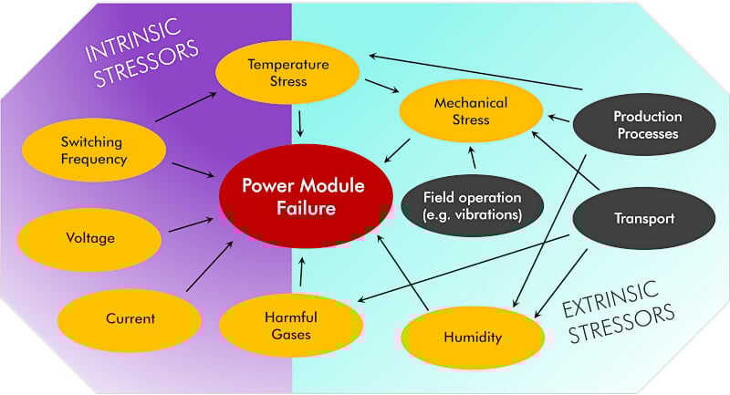
Figure 1. Common stressors affecting power electronics reliability. Image used courtesy of Bodo’s Power Systems [PDF]
Dendritic Structures after Field Stress or Qualification Tests
Particularly when moisture interacts with the module, typical failure mechanisms are triggered, which can lead to the formation of dendritic structures. These structures develop between the applied potential difference and can grow on the surface within a moisture film formed by condensation, or also within a polymer material that is exposed to moisture and has absorbed a sufficient amount of water into the bulk material.
On the one hand, as previously described, this can occur due to moisture stress in the field; on the other hand, a corresponding H3TRB (High-Temperature High-Humidity High-Reverse-Bias) test during product validation and qualification (see AQG324) can also trigger this stress and provide an indication of the module’s moisture robustness under humid environmental conditions in the field.
Especially in high-voltage applications, dendritic structures are usually found within a polymer material or along the interface between, for example, the insulation material and the substrate or chip surface. These structures are very easy to detect in the insulation trenches of silicone-encapsulated power modules, as they offer excellent optical accessibility. Nevertheless, although more difficult to observe, dendritic structures after moisture and high-voltage stress can also be found in other insulation systems, such as epoxy mold compounds, coatings, or in the case of embedded components [1, 2], in areas of the corresponding FR4 circuit board structure, such as the epoxy base material or the solder resist (Figure 2).
The dendrites may initially represent a purely optical anomaly and not lead to any electrical irregularities or changes in the module’s functionality. This is especially the case when the insulation distance between the dendritic structure and the opposite potential is still sufficiently large, or when minimal leakage currents or low resistances have no significant impact on the electrical functionality of the entire module. Typically, these leakage currents manifest as slight drifts in the corresponding H3TRB curves over the 1000 h testing time.
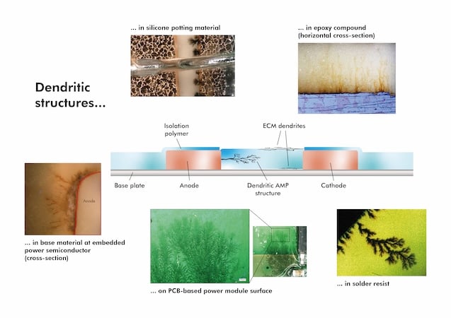
Figure 2. Dendritic structures in various polymer systems after humidity stress in the field or during qualification testing. [1,3-6]. Image used courtesy of Bodo’s Power Systems [PDF]
However, if there is no significant or sudden decrease in resistance – particularly below the specified limit – these effects are often given only minor attention, and the test is considered passed. The occurrence of dendrites between insulation trenches in the field often remains unnoticed until a sufficient reduction of the insulation distance occurs, leading to electrical irregularities or malfunctions that necessitate further investigation and disassembly of the module. The failure characteristics in such cases are very diverse. They can range from purely leakage current behavior to thermal events (thermal runaway), or to a voltage breakdown in the area of the bridging dendritic structure in the isolation trenches at sufficiently high voltages (Figure 3).
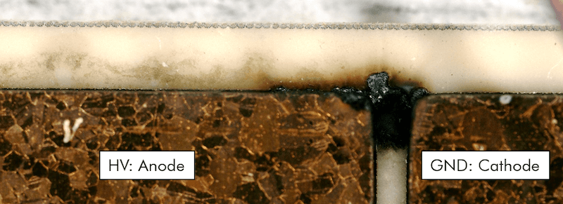
Figure 3. Voltage breakdown after partial bridging of the isolation trench by migration products. [3]. Image used courtesy of Bodo’s Power Systems [PDF]
Failure Mechanisms Behind the Phenomenology
Dendritic structures formed through corresponding moisture exposure under the respective potential difference (DC or AC with a corresponding DC component) on surfaces or within polymer materials are visually very similar. However, upon closer examination and with the background of the knowledge about the electrical wiring of the system, it is noticeable that dendrites growing on the surface are usually of a cathodic-anodic nature. In contrast, most dendritic structures within a material tend to originate from the anode side. Additionally, the times until failure – i.e., the formation of a conductive path or filament – are significantly shorter for cathodic-anodic grown dendrites (minutes to hours along surfaces) than for anodic-cathodic structures (weeks to years typically within polymer bulk material).
When examining the underlying mechanisms of these phenomena, it becomes clear that electrochemically, the same processes occur; however, external influences are decisive for the actual manifestation of the phenomena. Particularly, the material properties of the insulation system, the potential difference, and its magnitude are typical external influences.
The “standard” dendrite growth from cathode to anode on surfaces, characterized by the formation of a metallic dendrite, is referred to as electrochemical migration (ECM). ECM requires a water film with an applied electrical potential (> 1.5 V). For this mechanism to happen, only a few monolayers of water molecules are sufficient. When the water film connects the electrical potentials (DC), the anode material dissolves. The produced metal ions migrate to the cathode, where the reaction back to the metal occurs. The produced dendrite grows from the cathode back to the anode, creating a conductive connection [3, 4].
Anodic Migration Phenomenon
In contrast, the occurrence of dendritic structures within the bulk material of polymer substances – primarily exhibiting an anodic-cathodic growth direction – is referred to as an Anodic Migration Phenomenon (AMP) [3, 4, 7]. In the case of AMP, the chemical reactions and migration processes described for ECM occur in channels within polymer materials (insulation materials, mold compounds, conformal coatings, underfill, etc.) that connect the anode and cathode.
However, these channels may be formed by aging or degradation of the respective polymer material, caused by stressors such as high voltage, high temperature, or temperature changes and humidity, often combined with quality tolerances in the polymer material [5]. At high humidity, these channels between the anode and the cathode are filled with water. Metal cations released from the anode then begin to migrate within the channels toward the cathode. Since there is a gradient from the acidic to the alkaline pH (caused by electrolysis reaction of water in the presence of an electric potential), the ions precipitate at the pH boundary (acidic/alkaline) within the channels, forming a metal hydroxide deposit from the solution. The visual appearance of these channels filled with deposits resembles dendrites that begin to grow from the anode [3, 4].
AMP predominantly occurs in areas with high electric field strength (edges, tips, roughness, etc.), as these are most susceptible to partial discharges. Consequently, polymer degradation begins there. Additionally, the aforementioned quality variations in polymer materials, mostly caused by process tolerances, such as porosity, low degree of cross-linking, weak adhesion, or delaminations, increase susceptibility to partial discharges, and this leads to accelerated aging and degradation of the polymer matrix [3, 5].
How To Avoid Module Failures or Deal with Them
The susceptibility to AMP failures and thus the reliability of the power module or the entire system is primarily determined by the type of insulation material used. Although the material is selected during the design phase based on the expected mission profile and the corresponding stressors (both extrinsic and intrinsic), the selection is mainly made based on existing datasheets, material properties, and previous experience.
Within the field of failure analyses that Zestron performed over the past years, the company found out that these failures are rarely due to incorrect material selection of the insulation materials. Instead, failure analysis indicates that most AMP failures are caused by defects in the polymer material (coatings, potting, moldings, base material, solder mask, etc.), which were triggered by the application process itself or previous manufacturing steps.
For module suppliers, it is important to note that the parameters provided by the manufacturers are obtained under standard conditions and for specific process parameters (curing, layer thicknesses, mixing ratios, etc.) for each material. However, the mass production material properties (such as dielectric strength, mechanical stability, CTE, etc.) often change significantly when deviating from the ideal or specified process conditions. Thus, there can be a substantial difference in material quality when transitioning from prototype production to series manufacturing.
Developments in the field of e-mobility and the increasing efforts to integrate components and semiconductors into FR4-based PCBs (embedded components) also demonstrate that transferring these to higher stress conditions – particularly higher voltages – is not a straightforward 1:1 process, even though manufacturers have years of experience with corresponding materials and processes.
Process Stability at the Module Supplier Enables Reliability
Ensuring the reliability of a power module, especially under challenging operating conditions, the application and curing of the used polymer material is important. To gain the maximized performance of the material according to the datasheet specification, the adoption of the datasheet parameters to the individual, especially geometric, conditions is key (according to datasheet specifications).
The most critical parameters here are primarily the degree of crosslinking and the adhesion of the polymers to the respective substrate. From a process perspective, besides the application process itself (considering the specific component geometries), the curing process and the surface to be coated, potted, molded, or laminated are decisive (Figure 4). The latter is significantly influenced by the preceding manufacturing steps (such as soldering, sintering, etc.). Also, subsequent process steps like large area sintering or soldering, e.g., on a cooling base plate, may cause or enhance delamination effects caused by additional thermo-mechanical stress.
In addition to the interplay of these factors, especially during series ramp-up and ongoing production, it is essential to ensure that the optimal process conditions are maintained throughout the entire process chain. The final key to achieving moisture robustness of the power module is therefore continuous process monitoring by control of the insulation material quality.
Module Selection and System Design
In addition to the quality of the materials used and their interaction within the power module itself, it is often worthwhile to also consider the overall system. Besides the intrinsic moisture robustness of the module (discussing material selection and their combination), the system also plays a role in determining the extent to which moisture can access the module. A key factor here can be the enclosure design, which is crucial in preventing moist ambient air from reaching the module. This begins with the question of whether moisture-permeable membranes are used in the enclosure, allowing any ingress moisture to escape rather than accumulate, up to considerations of ventilation and air flow management.
Are there areas where laminar flow is absent, and moist ambient air is preferentially directed toward the module? Or could turbulence in the airflow actually reduce overall humidity within the system?
Additionally, it is important to identify the heat-carrying masses within the system as well as components that preferentially absorb or adsorb moisture (considering the material itself and possibly enhanced by hygroscopic contaminants from soldering or sintering processes). In some cases, simply changing the direction of airflow during ventilation can be sufficient, since forcing air through an enclosure often causes more turbulence than sucking air through it.
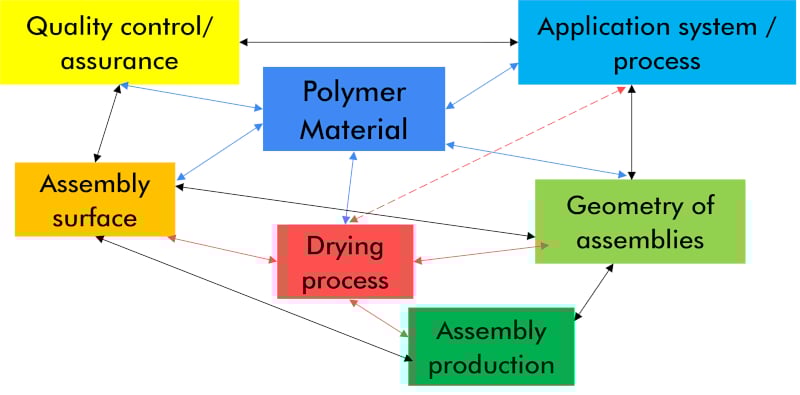
Figure 4. Influences on the polymer quality. [5]. Image used courtesy of Bodo’s Power Systems [PDF]
The measures and considerations mentioned above to achieve a reliable system can be discussed and implemented by the system supplier. From the supplier's perspective, there is no direct influence on the power module itself or its quality and reliability. Therefore, it is their responsibility to select a suitable module based on operational requirements in the field and the aforementioned mission profile. Always having in mind that not all eventualities during operation can be covered, the system manufacturer needs to ensure compliance with the operating conditions and limitations specified by the module manufacturer for each module.
Potential restrictions and maximum conditions in the field on the system level should be clearly communicated here. Nonetheless, due to the previously mentioned process variations, there are quality differences among various modules. To assist in module selection, appropriate qualitative tests can be applied, which provide indications of potential vulnerabilities in the field under stress conditions (moisture, harmful gases, thermal, mechanical, voltage, etc.).
Quality Check – Fast Pretesting
A crucial aspect is to question the extent, location, and timing of moisture or harmful gas ingress into the critical structures of the module (such as metallizations, chips, bond wires, etc.). The factors to examine include the degree of crosslinking and the homogeneity of the polymer network, as well as defect-free bonding and adhesion to the respective substrate surfaces. Susceptibility to AMP and partial discharges can be triggered by delaminations, porosity, or insufficient integration of fillers into the polymer matrix.
To support the selection of modules based on the preliminary preselection made by the system manufacturer, rapid quality tests such as the high-voltage “Coating Reliability Test” (CoRe test) according to IEC PAS 61191-10 can be helpful. Zestron currently applies this test up to 800 V. In this test, the module is subjected to water, representing a worst-case scenario to uncover potential weaknesses without claiming to predict the module’s lifespan. By monitoring possible leakage currents of different modules over a test duration ranging from several hours to a few days, significant quality differences can be effectively identified.
For comparative testing of power modules regarding delaminations, network inhomogeneities, and penetration paths for moisture and harmful gases, a quality test based on iodine vapor can be used [4, 6]. This is a multimodal, highly accelerated stress test (HAST) that simultaneously applies stressors such as moisture, harmful gas, and temperature. Due to this combined stress environment, the test duration can be significantly shortened. An initial pre-selection of modules for subsequent qualification testing (e.g., according to AQG324 via H3TRB) can be completed within a few hours. Besides saving time and reducing the duration of optimization cycles, this approach can also substantially lower development costs.
Stress Influences Effects on Functionality
Does the applied stress influence the functionality of the module or the electrical circuit? This fundamental question remains when analyzing and interpreting the results after quality testing, as well as exposure to any stress (H3TRB testing, vibration, mechanical shock, etc.). It brings the initially and currently in the community debated issue back into focus, whether an optically visible dendritic structure in the insulation trench after H3TRB testing or field stress constitutes a problem, even if no obvious electrical anomalies are observed in the circuit characteristics or electrical functionality.
One way to judge these optical or covered electrical irregularities more sensitively is through impedance spectroscopy (EIS) for module evaluation. Zestron has gained experience with this approach, performing impedance spectroscopy not as an absolute measurement but in a comparative manner – measuring before and after stress exposure (Figure 5).
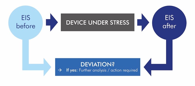
Figure 5. Procedure of test evaluation supported by impedance spectroscopy (EIS). Image used courtesy of Bodo’s Power Systems [PDF]
This method allows even minor changes in the impedance profile to indicate early signs of creeping currents or low-impedance pathways in the system, thus revealing potential module deficiencies under continued stress. Depending on which contacts are measured, it can also provide indications as to whether the weaknesses are more likely located on the chip side, at the interface between the chip and the insulation material, or within the insulation material itself. In many cases, the impedance profile can also predict which weaknesses are to be expected. For example, delamination effects and water ingress in polymer systems influence the impedance curve differently.
Literature
[1] A. Brunko, M.R. Meier, M. Gloth, N. Kaminski, “Embedded systems and printed circuit boards as weak spots in HV-H3TRB tests,” Microelectronics Reliability, vol. 138, pp. 114687-114691, 2022.
[2] Till Huesgen, Ankit Bhushan Sharma, Vladimir Polezhaev, “Leiterplatten embedding von Leistungshalbleiterbauelementen Stand der Technik und aktuelle Herausforderungen,” Symposium Elektronik und Systemintegration (ESI 2022), Landshut, 2022.
[3] M.R. Meier; H. Schweigart, “Corrosion in Power Electronics,” Proceedings of CIPS 2022 Conference, pp. 404-408, Berlin, 2022.
[4] M.R. Meier; H. Schweigart, “Iodine vapour based quality test for coating and potting materials of (power) electronic devices,” Microelectronics Reliability, vol. 150, pp. 115104-115109, 2023.
[5] M.R. Meier; H. Schweigart, “Protective coating of electronics – Defect root causes, failure mechanisms and quality evaluation tools,” Proceedings of SMTA Europe Electronics in Harsh Environments Conference, Amsterdam, NL, 2023.
[6] M.R. Meier; H. Schweigart, “Highly accelerated multi modal quality testing of conformal coatings, pottings and polymer lmaninates based on iodine vapor,” Proceedings of SMTA Europe Electronics in Harsh Environments Conference, Amsterdam, NL, 2025.
[7] Lux K, et al., Humidity induced failure mechanisms of electronic printed circuit boards (PCBs) during high voltage load, SMTA Electronics in Harsh Environments Conf. Proceedings, Amsterdam, 2018.
This article originally appeared in Bodo’s Power Systems [PDF] magazine.