Facebook
 Google
 GitHub
 Linkedin
Enabling Smarter DC Link Discharge in EV Traction Inverters
By using an integrated gate driver for DC link discharging, you can shrink BOM costs, save PCB space, and simplify your EV powertrain design.
This article is published by EEPower as part of an exclusive digital content partnership with Bodo’s Power Systems.
Discharging high-voltage DC link capacitors in automotive inverters typically requires bulky, costly external components impacting significantly the bill of materials (BOM) cost (estimated $4–$6 per inverter), consuming valuable PCB space, and complicating the design—particularly in compact and cost-sensitive EV powertrain applications.
NXP’s GD3162 gate driver introduces a highly integrated solution, reshaping how system designers approach discharge strategy by embedding it directly into the gate driver IC—enabling leaner designs, reducing BOM, and paving the way for advanced diagnostic and control strategies.
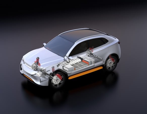
Image used courtesy of Adobe Stock
DC Link Discharge Challenges in Inverter
High-voltage DC links are central to a wide range of power electronic systems in electric and hybrid vehicles—including inverters relying on large capacitors (e.g 1 mF) to stabilize the voltage, reduce ripple, and support efficient control and operation. However, in the event of a malfunction or emergency—such as a crash or unexpected shutdown—the energy stored in these capacitors must be safely discharged to prevent human electrocution during car maintenance and in repair scenarios or first responders in crash. In this context, the automotive standard LV123 defines strict requirements for DC link discharge. It mandates that the voltage on the DC link (up to e.g 950 V) must be reduced to a safe level (typically below 50 V) within defined time limits: using passive discharge within 2 minutes and active discharge within 2 seconds.
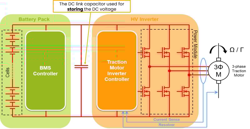
Figure 1. High-Voltage EV Powertrain Architecture. Image used courtesy of Bodo’s Power Systems [PDF]
Conventional active discharge systems often utilize resistive elements or PTC devices, either switched or thermally triggered, to dissipate the energy. These solutions, while effective, come with several drawbacks. For instance, PTC-based systems might need significant cool-down time (often 2 to 10 minutes) before they can be safely reactivated, limiting their suitability for repetitive or fastacting events. Additionally, resistors designed for continuous operation must be dimensioned for worst-case conditions—adding cost complexity, and space challenges.
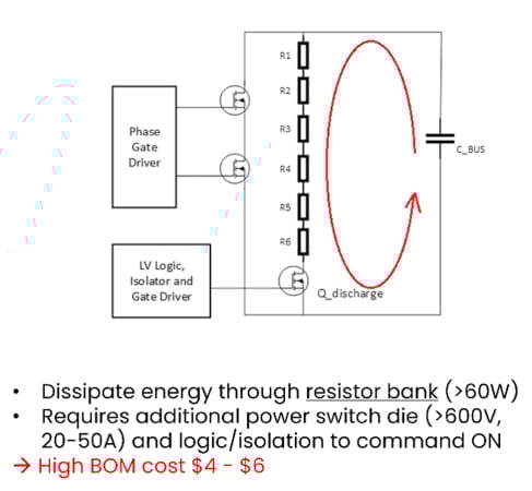
Figure 2. Conventional active HV bus discharge methods. Image used courtesy of Bodo’s Power Systems [PDF]
Integrated Discharge: A New Paradigm for Inverter Design
The GD3162 represents a shift in power electronics system design to address active discharge. Rather than externalizing the discharge function, NXP has integrated it within the gate driver, leveraging the existing power transistors of the inverter itself. This system-level approach eliminates the need for external components dedicated solely to discharge, reducing BOM while freeing up space for other critical components.
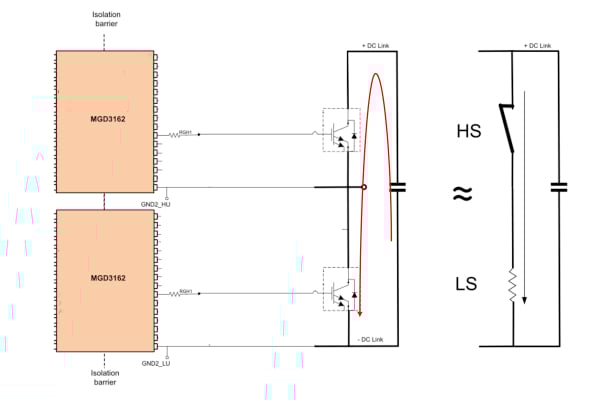
Figure 3. GD3162 DC Link Discharge operation. Image used courtesy of Bodo’s Power Systems [PDF]
The graph below illustrates the controlled discharge of a 950 V, 635 µF DC link capacitor using a SiC power module and the GD3162 gate driver.
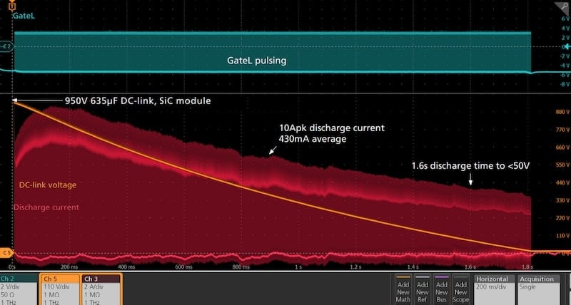
Figure 4. Demonstration of active DC Link Discharge using GD3162 Gate Driver. Image used courtesy of Bodo’s Power Systems [PDF]
The integrated discharge function is more than a cost-saving measure—it’s a platform enabler. With fewer components, designers can build more compact inverters, simplify system layout, and reduce failure points. The embedded intelligence also enables tighter coordination between safety functions, protection mechanisms, and diagnostics, which is crucial in automotive environments where functional safety and reliability are paramount.
System Benefits and Integration Considerations
From a system integrator’s perspective, adopting a gate driver with built-in discharge control brings numerous advantages. First, the simplified bill of materials reduces sourcing complexity and overall production cost. Second in addition, the GD3162’s design flexibility accommodates various system topologies. Whether used in SiC or IGBT-based platforms, the discharge function seamlessly integrates with the power stage. It also aligns with functional safety requirements, supporting ASIL levels through redundant monitoring, fail-safe modes, and self-diagnostic routines. This helps reduce the validation burden during automotive qualification and supports robust system-level FMEA.
Wolfspeed Collaboration: Validating Long-Term Reliability
To validate the power module lifetime impact of the GD3162 DC link discharge feature, NXP collaborated with Wolfspeed to evaluate the effects of repeated discharge on Wolfspeed’s EAB450M12XM3 SiC MOSFET power module. This test involved over 100,000 high-stress discharge cycles using a single phase setup under 800 V and 400 µF DC link conditions.
Despite the aggressive testing conditions— repeated discharge stress on the same die—Wolfspeed observed no measurable degradation in the SiC power module as illustrated on figure 5. These preliminary findings are encouraging and illustrate how a properly integrated discharge strategy can meet demanding automotive reliability standards without compromising performance.
Conclusion: Integration as a Competitive Advantage
The GD3162 offers a compelling new approach for designers of EV inverters, where every component must contribute to compactness, reliability, and cost efficiency. By embedding DC link discharge functionality into the gate driver, NXP not only streamlines system design but also provides pathways for enhanced diagnostics and improved safety compliance. More information on the GD3162 product page.
This is more than a component innovation—it’s a shift in how power systems can be architected for the EV era. As OEMs seek to differentiate on performance, reliability, and cost, intelligent integration at the semiconductor level will increasingly define the frontier of power electronics design.
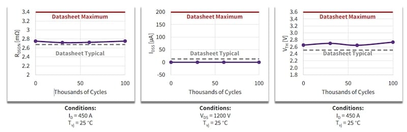
Figure 5. Wolfspeed’s EAB450M12XM3 SiC MOSFET parameters shift per discharge cycle at 25 °C. Image used courtesy of Bodo’s Power Systems [PDF]
To experience this innovation in action, visit NXP at PCIM Europe, Booth 5-430. Explore the live demonstration of the GD3162’s DC Link discharge feature and discover how NXP is enabling smarter, safer and more efficient EV systems through its latest portfolio of high voltage solutions.
This article originally appeared in Bodo’s Power Systems [PDF] magazine.