Facebook
 Google
 GitHub
 Linkedin
Dual Linear Regulator for Digital IC Power Enables On-the-Fly Output Adjustment and Dynamic Headroom Optimization
Low dropout (LDO) linear regulators are often used to provide clean power to processor cores and communication circuits. In these applications, LDO regulators are used specifically because processors and power amplifiers have stringent performance requirements for power supply output noise and load transient response. Often, these circuits demand an LDO regulator that is a good fit in terms of current rating and rails per IC in order to minimize solution size.
Typically, LDO regulators require hardware modifications to adjust their output voltage, but board and component changes can add significant development time if specifications are constantly changing. In such applications, an LDO regulator featuring a software programmable output voltage can save time and cost.
Nevertheless, software control of the LDO regulator output solves only part of the problem. LDO regulators are often used as a postregulator to a switching regulator. From the LDO regulator perspective, switching regulators are often used to preregulate input power before it reaches the linear regulator. Ideally, the output of the switching regulator has just the right amount of headroom— above the dropout voltage of the LDO regulator—so that the LDO regulator operates in its most efficient region, and transient response is optimized. To maintain the optimal input voltage to the LDO regulator, the output of the switching regulator must adjust with the LDO regulator’s output. Again, this is best accomplished without incurring costly hardware modifications.
The LT3072 dual 2.5 A linear regulator meets the challenging needs of digital IC power while allowing hardware-independent output voltage adjustments, even when the LT3072 follows a preregulator input supply. The LT3072 features UltraFast™ transient response and a low dropout voltage of 80 mV, allow it to easily produce tightly regulated supply voltages when loads change quickly.
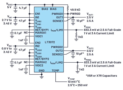
Figure 1. The UltraFast load transient response, 12 µV rms output noise, and 80 mV dropout voltage features of the dual-channel, 2.5 A LT3072 meet the needs of digital ICs with stringent power requirements. In this schematic, the three-state VO1B2–0 and VO2B2–0 pins are shown fixing OUT1 to 2.5 V and OUT2 to 0.6 V, respectively, but the output voltages can be changed simply by changing the states on those pins, enabling software control of the LT3072 without time-consuming and costly hardware modifications. Image used courtesy of Bodo’s Power Systems.
The low 12 µV rms output noise and UltraFast transient response of the LT3072 are attained with only 10 µF (1 µF + 2.2 µF + 6.8 µF) of output capacitance. Low noise is important for communication or sensor circuits to maintain their high performance.
The LT3072 incorporates two fully independent 2.5 A LDO regulators in a single package. The 0.6 V to 2.5 V output voltage range of the LT3072 is wide enough to power a wide range of digital IC rails. The output voltage for each channel is programmed by setting a few three-state pins on the LT3072—a method that can easily be performed via jumpers, a microcontoller, or a power system management (PSM) IC.
Programmable Dual Outputs with Low Noise and UltraFast Transient Response
Figure 1 shows the LT3072 in a standalone circuit suitable for digital IC loads with stringent power requirements. One important component of tight supply specifications is the ability to respond quickly to load transients, as illustrated by the LT3072’s UltraFast transient response shown in Figure 2.
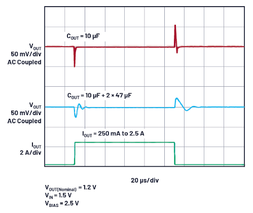
Figure 2. The UltraFast transient response for a single output of the LT3072 shows settling within microseconds with only 10 µF (1 µF + 2.2 µF + 6.8 µF) of output capacitance. The middle trace shows additional capacitance can be used to limit the excursion amplitude, but with a slightly longer settling time. Image used courtesy of Bodo’s Power Systems.
Each output value is programmed by three three-state pins: VO1B2, VO1B1, and VO1B0 and VO2B2, VO2B1, and VO2B0. Each three-state pin is set by either grounding, floating, or applying a voltage to it. In this way, the outputs can be programmed from 0.6 V to 2.5 V.
In addition to setting the nominal programmed voltage, margining inputs allow an additional ±10% adjustment around the programmed output voltages. The respective input voltages can be as low as 200 mV higher than the 2.5 V and 0.6 V output voltages, or slightly higher, in order to optimize headroom for transient response performance. Output voltage status is indicated by PWRGD pins, and there are pins for analog monitoring of output current that also program a ±7% accurate output current limit. There is a pin for analog monitoring of die temperature as well.
Dynamic Control of the Preregulator
The LT3072 can dynamically control the output of the switcher that precedes it. This enables on-the-fly adjustments of an LDO regulator’s output voltage while maintaining its input voltage at a level that maintains high efficiency and fast load transient response.
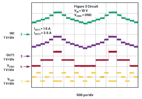
Figure 4. Dynamic test of the circuit in Figure 3. Traces show how software-applied changes to the three-state pins, VO1B2 and VO1B1 (VO1B0 grounded), result in the voltage adjustments at OUT1 of the LT3072. The LT3072, in turn, dynamically controls the LT8616 Channel 1 output, which preregulates the LDO regulator’s IN1 input. In this way, the voltage at the LDO regulator’s IN1 remains a fixed amount over the LDO regulator’s OUT1—a voltage difference that results in the highest efficiency and best load transient performance—all without any changes to hardware. Image used courtesy of Bodo’s Power Systems.
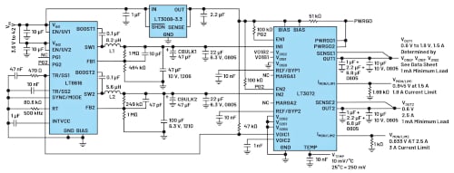
Figure 3. IN1 and IN2 of the LT3072 are preregulated by the dual-channel, step-down LT8616. The connection between VOIC1 of the LT3072 and TR/SS1 of the LT8616 allows the LT3072 to dynamically preregulate its IN1 input, resulting in the highest efficiency and load transient performance, while allowing adjustments to the LT3072 output voltage without hardware changes. Image used courtesy of Bodo’s Power Systems.
The preregulator supply for the LT3072 in Figure 3 is the LT8616—a 42 V, dual 1.5 A/2.5 A synchronous monolithic step-down regulator. This setup can accept a single 3.6 V to 42 V system input voltage range. In this solution, the programmable output range of the LT3072’s OUT1 is from 0.6 V to 1.8 V. The OUT1 channel uses VIOC to control the corresponding LT8616 output to keep the LDO regulator working in an optimal efficiency and transient response conversion region. OUT1 can be adjusted dynamically from 0.6 V to 1.8 V using the VO1B2-1 pins.
Current limit for the OUT1 linear regulator channel is set to 1.8 A, which is slightly higher than the 1.5 A maximum output current of the LT8616 Channel 1. OUT2 is fixed at 0.6 V, capable of 2.5 A with a 3 A current limit.
The LT3008-3.3 provides BIAS to the LT3072. The PG2 (power good) pin of the LT8616 provides a slight delay before startup of the LT3072. Figure 4 shows the LT3072 dynamically controlling the switcher channel that preregulates the LDO regulator input.
Conclusion
The LT3072 dual LDO regulator for digital IC power features two low noise channels with UltraFast load transient response. The two output voltages are programmed by setting a few three-state pins—no resistors required. When the input supply to the LT3072 is a preregulator, the LT3072 VIOC function can be used to control the input supply to allow dynamic changes in output voltage programming without sacrificing transient response performance or efficiency.
About the Author
Andy Radosevich is a senior applications engineer with Analog Devices, supporting Power by LinearTM nonisolated, dc-to-dc switching, and linear voltage and current regulators. Andy received an M.S.E.E. from San Jose State University, specializing in power electronics. He also has a background in motion control and light to medium manufacturing processes. Andy is an avid public transportation commuter and often takes the bus to Silicon Valley engineering events.

Image used courtesy of Bodo’s Power Systems.
This article originally appeared in Bodo’s Power Systems magazine.