Facebook
 Google
 GitHub
 Linkedin
Digital Power Supply Loop Design StepbyStep Part 1
This article highlights Ali Shirsavar practical techniques for digital PSU control loop design to help engineers stabilise their digital control loop.
Designing digital power supply control loops is surprisingly easily. The reason for the mystique may be that even though we study all the necessary techniques at university, unfortunately they are often taught only at great theoretical depth. The theory however, is rarely applied to real life circuits such as a power supply, often making the task intimidating.
In this article, and subsequent ones, we will present easy to follow, practical techniques for digital PSU control loop design to help engineers stabilise their digital control loop. These are some of the techniques that are a taught in Biricha’s Digital Power Supply Design Workshops [1].
Introduction
One point that we should stress at the onset is that there is nothing scary about digital control loop design; all we are doing is using a microprocessor to solve a single mathematical equation.
In the analog world, we design our control loops using operational amplifiers. Operational amplifiers also solve mathematical equations. The trick is to create an equation in the digital domain that gives us the same answer that we would get out of our operational amplifier. You will see in the course of this article that the gain output of almost “any” analog op-amp with a known transfer function can be replicated very accurately in the digital/discrete domain with a single equation. There will be some discrepancy in the phase plot of an analog op-amp’s transfer function with respect to its digital counterpart, but we will deal with that in a later article.
As suggested in previous Biricha Articles in this magazine, most analog PSU compensators are either a Type II or Type III op-amp circuit [2],[3]. Therefore, all we have to do is to convert the transfer functions of each one of these op-amp circuits into a single discrete time/digital equation.
Digital Power Supply Building Blocks
In the next figure, we have shown a standard digital power supply where the op-amp has been replaced by an ADC and a digital compensator called Hc[z] which, as mentioned earlier, is just a single equation. For now, let us ignore what this equation is and instead concentrate on what happens in a digital power supply in a step-by-step manner.
Please note that we are operating on numbers that are sampled by the ADC and there-fore we only know these numbers whenever we have the sample; this is called “Discrete Time”. For example, if our switching frequency is 200kHz and we sample the output voltage once per cycle, then every 5μs (i.e. 1/200kHz) we know the output voltage.
So starting from the left hand side of our PSU figure, we have our output voltage Vout in volts plotted with respect to time as shown on Plot A. Therefore, every 5μs. i.e. at a rate of 200kHz, our ADC samples Vout, giving us Plot B. Plot B is a digitized representation of our output voltage.

Figure 1: Digital PSU Building Blocks
You will see from Plot B that when n = 0, i.e. at time t = 0μs we have a sample from the ADC, then 5 μs later i.e. when n = 1 or at t = 5μs we have a second sample, then 5μs later we will have our 3rd sample and so on. Therefore, Plot B is our Vout plotted with respect to sample number n.
Ignoring all our scalings for now (we will deal with these later) and assuming that we would like an output voltage of 3.3V, then we have Plot C. In this plot, we show the voltage that we would like to have at every sampling interval. In other words, when n = 0, i.e. when t = 0 μs, we would like to have 3.3V on the output. Then, 5μs later i.e. when n = 1 (so t = 5μs), we would like 3.3V on the output, then 5μs later, again we want to have 3.3V on the output and so on. This is our reference or demand voltage Vref[n] plotted with respect to sample number.
Now, if starting at t = 0, at 5μs intervals, we subtract the voltage the ADC says we have on the output, i.e. Vout[n], from the voltage that we actually want on the output Vref[n] then the difference between these two is our error Verror[n]. This signal is the input to the controller which for simplicity from now on we will call x[n]. We have shown this on Plot D.
Digital equivalent of an op-amp compensator.
Now that we have our error signal, we can compensate for it using a digital equivalent of an op-amp compensator. As mentioned earlier, this is just a single equation. The output of this equation y[n] at every sampling interval is a near exact replica of the output of the equivalent op-amp compensator and sets the new value of our duty. Note that for now we are ignoring the scalings and any phase delay due to digitization; we will deal with these later articles.
Finally, the output y[n], i.e. our demand duty is fed into the digital PWM block as shown which will then turn ON the switch. You can see that we have closed our loop. Provided that we can derive a discrete time mathematical equation that gives the same output as the op-amp compensator then our digital power supply should, in theory, behave just like the analog one.
Can an Equation in Discrete Time/Digital Domain Give the Same Output as an Op-Amp?
Yes it can! It is done by using something called a “Linear Difference Equation” or LDE. In fact almost any continuous time/Analog transfer function can be converted into a near equivalent digital version using LDEs.
Here is an example of a discrete time linear different equation:y[n] = x[n] + 0.5 y[n-1]
There is nothing scary about LDEs, in fact they are very very easy to calculate. We just need to spend a few minutes discussing what all the “n”s in the square brackets mean.
y[n] means the output of our digital controller at this exact instance. This is the value that updates our duty and should be exactly the same as the output of our equivalent op-amp circuit, ignoring all the scalings and phase losses for now.
x[n] is the input to our digital controller at this exact instance. As discussed earlier, this is simply our error signal, i.e. the difference between the Vout that we want and the Vout that we are actually getting.
Then we have a coefficient of “0.5” multiplied by y[n-1]. Every time we see a y[n-1], it means our “previous” output, i.e. the output of our controller delayed by 1 sampling interval, or, in other words your output 5 μs ago. So 0.5 y[n-1] means half of our last output from 5μs ago. Of course the microprocessor know this value because we have the value of y[n] from 5μs ago.
If we see a y[n-2], it means our ‘Previous Previous’ output; in other words the output of our controller 10μs ago. y[n-3] would mean our output 15 μs ago and so on. Similarly x[n-1] means our previous input and so on.
Therefore, all we need to get the LDE to give the same output as an op-amp is to fill in the correct sample values in the LDE, multiply by the correct coefficient and then sum them up to get the new value of y[n] which sets our duty.
Let us use a real life example to put these in perspective. Consider the simple op-amp integrator shown in the next figure. This has a pole at origin and can be considered to be a Type I compensator.
If we solder a 1.6kΩ resistor for R and a 10nF capacitor for C then our gain plot will cross the zero dB axis at 1/(2π R C) = 10kHz. From previous articles [2] and Biricha workshops [3], we know that the Gain Plot of this circuit will look like the red trace figure shown below. You

Figure 2: Simple Op-Amp Integrator
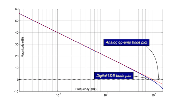
Figure 3: Gain plots of our op-amp integrator and its equivalent digital LDE
can see from this figure that the red trace crosses the zero dB axis at 10kHz.
But what about the equivalent digital Linear Difference Equation? Well, the equation below is our digital equivalent LDE. We will talk about how we derived this later but for now let us see if there are values within this equation that we do not know.
We can calculate y[n]; i.e. the controller output at this exact sampling interval. This is the output of our LDE which sets our duty and should be numerically equivalent the output of our op-amp circuit. We calculate this every sampling interval.
We know x[n]; our current input at this exact sampling interval. This was the input to our controller, which in our case was the error signal.
Of course, we also know both x[n-1] i.e. our previous input from 5ms ago and y[n-1] i.e. our previous output from 5ms ago.
Finally, we can see that our current input x[n] and our previous input x[n-1] are multiplied by the same coefficient (-Ts/2RC).
We know that R = 1.6kΩ and C = 10nF and let us assume that our sampling frequency is 50kHz and hence Ts = 20us.
Calculate the coefficients of both x[n] and x[n-1] -> -20us/(2x1.6kΩx10nF) = -0.625.
By substituting -0.625 into our linear difference equation becomes:
y[n]=−0.625x[n]−0.625x[n−1]+y[n−1]
Looking back at the gain plot of our op-amp, you will see that we have superimposed the output of this equation in frequency domain on top in blue. As you can see, we have a near-perfect match and we have successfully created a digital compensator/LDE with a gain frequency response that is almost exactly the same as that of an analog op-amp.
We should point out that for teaching purposes we reduced our sampling frequency down to 50kHz to show some discrepancy! If we were sampling at 200kHz we would barely be able to tell the difference until we approached the Nyquist frequency. Provided that we keep our compensator’s crossover frequency less than 1/20 of our sampling frequency, we can have a near perfect match in digital world compared to analog.
How Do We Derive LDEs?
The equation in this article was derived using the Bilinear Transform. Although there are other methods, the Bilinear Transform is a very common technique used to convert analog transfer functions into digi-tal format. There is nothing complicated about it; it just requires a little bit of algebra to go from a transfer function in Laplace domain to a discrete time LDE. The good news is that because the vast majority of power supplies in the Analog world are stabilised with either a Type II or a Type III, you may not need to learn the Bilinear Transforms at all. All you need is the LDEs for the Type and Type III and we will provide you with both of these simple equations in forthcoming articles.
These two equations (one for Type II and one for Type III) should cover many applications; however, for those who need to create their own high performance algorithms then we do cover the Bilinear Transforms in Biricha’s Digital Power Workshops for completeness.
Concluding Remarks
You can see from the previous discussions that that it is possible to emulate the output op-amp compensator with a single linear difference equation. In this article we demonstrated this fact using a simple op-amp integrator. However, nothing stops us from applying the same principle to Type II and Type III compensators.
In the forthcoming articles we will address all of the remaining issues and explain how to overcome them. We will present the LDEs that you need to create a digital version of a Type II compensator as used in most current mode power supplies as well as Type III, as applied to voltage mode.
We will discuss all scaling factors in detail with worked examples to show how to account for them. We will also discuss how to calculate and overcome the phase loss in a digital power supply. Finally we will carry out a detailed step-by-step design example for a real power supply and present real experimental results to verify the theory.
About the Author
Ali Shirsavar holds a Doctorate of Philosophy (Ph.D.) in Power Electronics at the University of Reading, Berkshire, England. He was an Associate Professor at the University of Reading for more than 17 years. He then became the Director of Biricha Digital Power.
This article originally appeared in the Bodo’s Power Systems magazine.
Related Content