Facebook
 Google
 GitHub
 Linkedin
Digital Electronics Basics: Universal Gates
Learn about basic logic gates that can be combined to implement any Boolean expression.
The OR, AND, and NOT are the three basic logic gates as they together can construct the logic circuit for any given Boolean expression. NOR and NAND gates have the property that they individually can be used to hardware-implement any logic circuit. For this reason, the NAND and NOR gates are called universal gates.
A Review of the Inverter or NOT Circuit
An inverter circuit reverses or complements the logic state applied to its input. Inversion is also termed the NOT operation.
The electromechanical circuit in Figure 1 – a battery-powered LED – shows how a NOT circuit operates. The solenoid R controls the normally closed switch a.
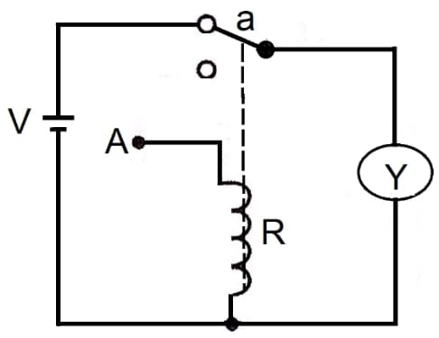
Figure 1. An electromechanical inverter or NOT circuit.
Initially, the only input to this circuit, A, has no connection to the battery, meaning a logic 0 signal (assuming positive logic). Under this condition, Y = 1 (logic 1), and the LED is on.
Connecting the battery to input A means logic 1. In this case, the battery energizes the solenoid R, which opens the switch a, blocking the current and turning the LED off. Under this condition, Y = 0 (logic 0).
Table 1 summarizes these results in a truth table.
| A | Y |
| 0 | 1 |
| 1 | 0 |
Table 1. The truth table for a NOT circuit.
Figure 2 shows the logic symbol and Boolean expression for the inverter or NOT gate.
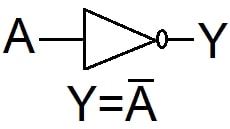
Figure 2. The logic symbol and Boolean expression for the inverter or NOT gate.
The NAND Gate
NAND stands for NOT-AND. A NAND gate is an AND gate followed by a NOT circuit – a negated output. This is one of the most useful combinations of gates.
Figure 3 is an electromechanical circuit showing the principle of a NAND gate.
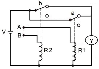
Figure 3. An electromechanical NAND circuit.
The battery supplies power to the LED through the normally closed switches a and b. The solenoid R1 controls switch a, and the solenoid R2 controls switch b.
Initially, inputs A and B are de-energized, meaning a logic 0 signal (assuming positive logic). Under this condition, the LED is on and Y = 1 (logic 1).
Connecting only the input A to the battery (logic 1), the solenoid R1 opens switch a, but the LED is still supplied through switch b and Y = 1 (logic 1).
Connecting only the input B to the battery (logic 1), the solenoid R2 opens switch b, but the LED is still supplied through switch a and Y = 1 (logic 1).
Finally, connecting both inputs, A and B (logic 1), the solenoids R1 and R2 open switches a and b, de-energizing the LED. Under this condition, the LED is off and Y = 0 (logic 0).
Table 2 summarizes these results in a truth table.
| A | B | Y |
| 0 | 0 | 1 |
| 0 | 1 | 1 |
| 1 | 0 | 1 |
| 1 | 1 | 0 |
Table 2. The truth table for a two-input NAND circuit.
The output of a NAND gate is a logic 0 when all its inputs are logic 1. For all other input combinations, the result is logic 1.
The NAND Gate Symbol and Boolean Expression
Figure 4 shows the circuit symbol and Boolean expression for a two-input NAND gate.
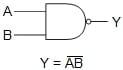
Figure 4. Two-input NAND gate symbol and Boolean expression.
The Boolean expression for a NAND gate with more than two inputs is
\[Y=\overline{ABCD}\]
Using a Combination of NAND Gates to Create Other Basic Logic Gates
Any logical function can be implemented by repeated use of the NAND circuit alone. Some examples follow.
Figure 5 shows a two-input NAND gate connected to create a NOT circuit. A single-input NAND is a NOT.
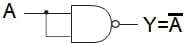
Figure 5. A NOT circuit made with a two-input NAND gate.
Figure 6 shows two NAND gates connected to create a two-input AND gate.
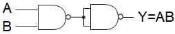
Figure 6. A two-input AND gate made with two NAND gates.
Figure 7 shows three NAND gates connected to build a two-input OR gate.
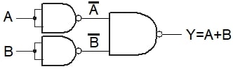
Figure 7. A two-input OR gate made with three NAND gates.
The NOR Gate
A negation following an OR is a NOT-OR or NOR gate.
Figure 8 is an electromechanical circuit showing the principle of a NOR gate.
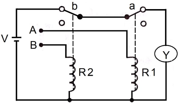
Figure 8. An electromechanical NOR circuit.
The battery supplies power to the LED through the normally closed switches a and b. The solenoid R1 controls switch a, and the solenoid R2 controls switch b.
Initially, inputs A and B are de-energized, meaning a logic 0 signal (assuming positive logic). Under this condition, the LED is on and Y = 1 (logic 1).
Connecting only the input A to the battery (logic 1), the solenoid R1 opens switch a, blocking the current and turning the LED off. Under this condition Y = 0 (logic 0).
Connecting only the input B to the battery (logic 1), the solenoid R2 opens switch b, blocking the current and turning the LED off. Under this condition Y = 0 (logic 0).
Finally, connecting both inputs, A and B (logic 1), the solenoids R1 and R2 open switches a and b, de-energizing the LED. Under this condition, the LED is off and Y = 0 (logic 0).
Table 3 summarizes these results in a truth table.
| A | B | Y |
| 0 | 0 | 1 |
| 0 | 1 | 0 |
| 1 | 0 | 0 |
| 1 | 1 | 0 |
Table 3. The truth table for a two-input NOR circuit.
The output of a NOR gate is logic 1 when all its inputs are logic 0. For all other input combinations, the outcome is a logic 0.
The NOR Gate Symbol and Boolean Expression
Figure 9 shows the logic symbol and Boolean expression for the NOR gate.
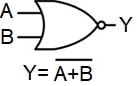
Figure 9. Two-input NOR gate symbol and Boolean expression.
Using a Combination of NOR Gates to Create Other Basic Logic Gates
All logic can be accomplished via the NOR circuit only. Some examples follow.
Figure 10 shows a two-input NOR gate connected to produce a NOT circuit. A single-input NOR is a NOT.
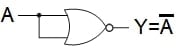
Figure 10. A NOT circuit made with a two-input NOR gate.
Figure 11 shows two NOR gates connected to create a two-input OR gate.
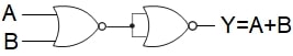
Figure 11. A two-input OR gate made with two NOR gates.
Figure 12 shows three NOR gates connected to build a two-input AND gate.
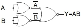
Figure 12. A two-input AND gate made with three NOR gates.
The Inhibit (Enable) Operation
This operation is functional when the transit of a logic signal needs to be either inhibited or enabled depending upon specific control inputs.
The circuit in figure 13 – a battery powering a LED – shows the working principle of the inhibit (enable) operation.
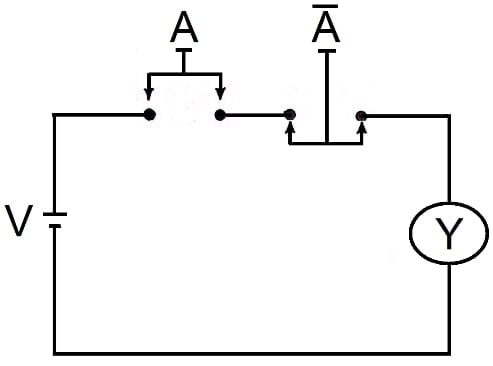
Figure 13. The inhibit (enable) operation.
The switch denoted A is normally open, and the switch marked Ā is normally closed. Pushing switch A will turn on the LED. However, when pushing the switch Ā, the circuit opens, and the LED cannot turn on when pushing both switches simultaneously. In this way, the switch Ā has an inhibit function in which A AND Ā = 0. Using the logical connection of the AND function, it can be expressed as A ∙ Ā = 0 (or A Ā = 0).
Table 4 is the truth table for this circuit (do nothing = logic 0, push switch = logic 1, Y = 0 LED off, Y= 1 LED on).
| A | Ā | Y |
| 0 | 0 | 0 |
| 1 | 0 | 1 |
| 0 | 1 | 0 |
| 1 | 1 | 0 |
Table 4. The truth table for the circuit in figure 13.
The Inhibit Symbol and Boolean Expression
The inhibit function can be implemented by adding an additional input to an AND gate. This additional input is negated by an inverter. The NOT circuit preceding the terminal S of the AND gate acts as an inhibitor.
Figure 14 shows the logic symbol and Boolean expression for an AND gate with an enable terminal (S).
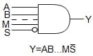
Figure 14. AND gate and Boolean expression with an enable terminal (S).
This circuit operates in accordance with the following logical statement: If A = 1, B = 1, …, M = 1, then Y = 1 provided that S = 0. A value of S = 1 forces the output to be at logic low Y = 0.
The Boolean equation reads: Y equals A AND B AND … AND M AND NOT S.
Table 5 shows the truth table for a three-input AND gate containing one inhibitor terminal (S). The enabling bit S = 0 lets the gate execute its AND logic, while the inhibiting bit S = 1 keeps the output at Y = 0, no matter what the values of the input bits are.
| A | B | S | Y |
| 0 | 0 | 0 | 0 |
| 0 | 1 | 0 | 0 |
| 1 | 0 | 0 | 0 |
| 1 | 1 | 0 | 1 |
| 0 | 0 | 1 | 0 |
| 0 | 1 | 1 | 0 |
| 1 | 0 | 1 | 0 |
| 1 | 1 | 1 | 0 |
Table 5. The truth table for a three-input AND gate, with one inhibitor terminal.
About Universal Gates
It is feasible to perform any Boolean expression using either only NAND gates or only NOR gates. For this reason, the NAND and NOR are universal gates.
The NAND and NOR gates are complements of the AND and OR gates. Their truth tables are the output states of the originals but reversed.
The circuit symbols are the same but with a small circle on the output, indicating the inversion of the logic level.
The Boolean symbols change by placing a bar over the original expression: AB becomes \(\overline{AB}\), A + B becomes \(\overline{A+B}\), and so on.
Adding a negated input to an AND gate can create the inhibit/enable functionality.
Featured Image used courtesy of LJ Create