Facebook
 Google
 GitHub
 Linkedin
Compact Active Clamp Flyback Design
Conventional flyback converters have a disadvantage due to the ringing caused by the transformer leakage inductance and the main switch parasitic capacitance resonance; this causes a high voltage stress on the switch. In addition, the leakage inductance energy is wasted in a passive clamp, such as most commonly used RCD snubbers, limiting converter efficiency and resulting in thermal dissipation.
An Active Clamp Flyback (ACF) architecture will recycle the flyback transformer leakage inductance energy as well as limit the voltage spike in the primary FET drain during turn-OFF periods. This article begins with a look back in history 50 years ago when the Flyback Converter architecture emerged in the power management design community. The article proceeds to dive into the technology of the Active Clamp Flyback architecture with a technical look at a new compact design by Silanna. Silanna's unique offering of fully integrated ACF controllers, such as SZ1110 and SZ1130, provides highly compact design in a 16-pin SOIC package. The IC has anOptiModeTM smart digital control that will adjust the operation mode on a cycle-by-cycle interval to maximize efficiency, keep EMI low, regulate the load dynamically and fast, as well as adjust to line load and voltage changes.
An all-silicon implementation of a 65W universal input AC/DC power supply achieves > 94% efficiency using SZ1130.
50 years ago, the Forward Converter entered upon the power management architecture scene. This design has dominated the commercial power supply arena, especially at the 50W power level.
In June of 1975, ‘your father’s ACF’ architecture started to take shape when Massey and La Duca presented an architectural solution that was to help optimize the power supply reset via the use of a voltage clamp. They were able to adjust the amplitude so that it provided the minimum necessary voltage during the converter’s reset interval.
Then, in 1981, Carsten employed an active clamp circuit using several variations. This provided an optimum reset voltage as the duty cycle goes through its changes and recovered most of the core energy, enabled symmetrical core excitation with low-loss switching transitions. Your father’s Active Clamp Flyback concept was born and thereafter virtually eliminated clamping and switching losses.
Changes since then have involved increasing switching frequencies from around 2 kHz to 500 kHz and higher. This was made possible mostly due to device improvements, packaging advances, and reduced size requirements. Isolated or non-isolated flyback topology is typically a key part of off-line converters with a power output spanning a few watts up to around 100 W. The architecture is based upon a single switch topology along with the energy taken from the input and stored in the transformer’s primary inductance while the power switch is switched ON, then that energy is transferred to the secondary output when the power switch turns OFF. Efficiency, power density and low stand-by power are the important requirements for flyback topologies along with its reliability.
The shrinking “Wall Wart”
The charger adapter, aka ‘Wall Wart’, operates as a typical switch-mode power supply (SMPS).The power converter function turns the FETon and off hundreds of thousands of times per second; this is known as the switching frequency. The higher the frequency is, the smaller the magnetics will be. We don’t want the switching frequency to be too high because that will cause problems:

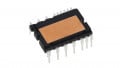
Figure 1: Silanna’s all-Silicon ACF IC combines four functions in one package
1. Transformer leakage inductance—each time the FET switches, energy gets stored in the transformer parasitic inductor and is then dissipated via the RCD clamp. But, if the switching frequency is too high, this would lead to excessive losses that could overheat the adapter. Active clamp comes to the rescue by using that leakage energy to improve efficiency. How? By storing it in a capacitor clamp, and later in the switching cycle, delivering it to the output.
2. By controlling the clamp with intelligence, Zero Voltage Switching (ZVS) is achieved at the FET, which in turn will increase the overall efficiency by reducing the switching losses. This will enable the designer to increase the switching frequency of the Active Clamp Flyback (ACF).
The ACF Advantage
In order control the ACF optimally, the controller will need to be intelligent and fast. Enter the Silanna, all-Silicon, SZ1110 (33W) and SZ1130 (65W) Active Clamp Flyback (ACF) PWM Controllers which integrate an adaptive digital PWM controller (Opti-ModeTM) and Ultra High-Voltage (UHV) components: Active Clamp FET, Active Clamp Gate Driver, and a Start-up Regulator. This IC solution creates the highest integration ACF controller. Figure 1.
Functional operation of Silanna’s Active Clamp Flyback (Figure 2)
ACF operation main advantages(Figure 3)
1. ACF reduces peak voltage and enables amore aggressive turns ratio to be implemented. The SR FET voltage rating can belower. ACF recycles leakage energy which,in turn, enables higher efficiency. Softswitching in the active clamp FET leads tolower EMI.
2. Active clamp leads to a lower QR valley,well under 200V with near ZVS of the mainswitch. This leads to higher efficiency because of lower switching losses and lowerEMI from smaller switching voltage.
The power supply contact points, shown in blue in Figure 4, benefit by the OptiMode™ feature by continuous monitoring of the following critical areas:
- Main switch adjustment on/off time performed cycle-by-cycle
- The ability to maintain high efficiency, lowEMI, line/load regulation, as well as otherkey parameters via continuous monitoring
- Optimization of system performance evenunder varying load/line/temperature

Figure 2: Active Clamp Flyback Operation steps

Figure 3: The main advantages of ACF
As a result, an all silicon implementation of a 65W universal input AC/DC power supply can achieve >94% efficiency and maintains a flat efficiency curve across varying load/line/temperature conditions.
OptiMode Also Provides:
- Highest efficiency via selection of optimal mode of operations
- Burst mode, adaptive valley switching mode as well as other proprietary modes
Fault Protection
SZ1110 and SZ1130 provide comprehensive list of fault protections, including Over Current Protection (OCP), Input and Output Over Voltage Protections (OVP), Over Power Protection (OPP), Internal and External Over Temperature Protections (OTP), etc. There are three versions of the SZ1110/30, each one has a different fault protection feature from which the designer can choose:
1. Part # SZ11XX-00 has Hiccup Mode Fault Protection for all faults
2. Part # SZ11XX-02 has Hiccup Mode Fault Protection (OTP latched)
Part # SZ11XX-03 has Latched Mode Fault Protection (Under-Voltage {UV} Auto-Recovery)Where, XX = 10 and 30 for Integrated ACF controllers supporting up to 33W and 65W output power applications, respectively. The IC packageThe 16-pin package has two pins removed: pins 2 and 5. Figure 5.

Figure 4: OptiMode™ enables adjustment of the contact points encircled in blue in the diagram
The IC packageThe 16-pin package has two pins removed: pins 2 and 5. Figure 5.

Figure 5: Pins 2 and 5 are removed from the package
The reason for this is that pins 1, 3, and 4 are Ultra High Voltage (UHV) pins that have absolute maximum rating of 620 V. Pins 2 and 5 were removed in order to meet the creepage requirement of those UHV pins, keeping the UHV away from the five to ten Volts low voltage pins. Pins 3 and 4 are able to be next to each other since the differential voltage between them is only six Volts maximum. Figure 6.
Reference Design Board
Reference board designs are available (with Gerber files upon request). There are also test reports available; those include BOM and comprehensive list of test results, such as efficiency, EMI, thermal measurements, and more.
We have come quite a long way from your Father’s ACF design, entering into the third decade of the New Millennium. As designers, we have markedly improved ICs, tools, and architectures that help us to shrink physical design sizes with component integration and higher frequency capability, demonstrating best-in-class efficiencies (> 94%) using an all-silicon implementation. High efficiency for better thermal performance, combined with Silanna Semiconductor’s ACF controllers’ high level of integration, enable high density and cost-effective power management solutions.
| Pin # | Name | Voltage Category (Vdc) | Description |
| 1 | CLAMP | UHV (620V) | Drain of Active Clamp (ACL) FET. Connect through a clamp capacitor to VBULK |
| 3 | SW | UHV (620V) | Switching node. Connect to transformer primary and Drain of the Primary N-FET |
| 4 | BOOT_CL | UHV (620V) | Bootstrap supply input for internal ACL FET driver. Connect a bootstrap diode from V5OUT to BOOT_CL and a bootstrap capacitor from SW node |
Figure 6: The SZ1110/30 high voltage pins
References
- The history of the Forward Converter, Rudy Severns, Switching Power Magazine, July 2000https://pdfs.semanticscholar.org/0911/34a5dc72c5a363ec937e40c0aa3706f1cd99.pdf
- Improved single-ended regulated DC/DC converter circuit, J. LaDuca, R.P. Massey, Power Electronics Specialists conference, June 9-11, 1975
About the Author
Ahsan Zaman received his Bachelor of Applied Science in the Field of Electrical and Electronics Engineering, Master's degree in Electrical and Electronics Engineer, and Doctor of Philosophy in Electrical and Electronics Engineering at University of Toronto. He worked as the director of product marketing at Silanna Semiconductor.
Aleksandar Radic received his Bachelor of Applied Science with Distinction in the Field of Electrical Engineering and Master's of Science in the Field of Electrical Engineering at the University of British Columbia, then PhD in the Field of Power Electronics at the University of Toronto.
Related Content