 Facebook
 Google
 GitHub
 Linkedin
CMOS implementation of XOR, XNOR, and TG gates
Learn how to implement the logic gates XOR, XNOR, and Transmission Gate (TG) using CMOS.
The CMOS family is the top choice for digital-logic design due to its many advantages. This article shows some logic gates implemented with CMOS.
The Exclusive OR Circuit (XOR)
In an XOR circuit, the output is a logic 1 when one and only one input is a logic 1. Hence the output is logic 0 when both inputs are logic 1 or logic 0 simultaneously.
Table 1 exhibits the truth table for an XOR circuit.
| A | B | Y |
| 0 | 0 | 0 |
| 0 | 1 | 1 |
| 1 | 0 | 1 |
| 1 | 1 | 0 |
Table 1. The truth table for an exclusive OR circuit.
A logic statement to express the XOR gate is as follows: If A = 1 and B = 0, or if B = 1 and A = 0, then Y = 1. In Boolean notation
\[Y=A\bar{B}+B\bar{A}\]
Figures 1 and 2 show two logic block diagrams to realize this function.
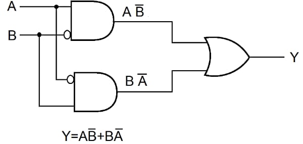
Figure 1. A logic block diagram for the XOR Gate.
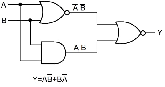
Figure 2. Another logic block diagram for the XOR Gate.
Figure 3 shows an implementation, in CMOS, of the arrangement of figure 2.
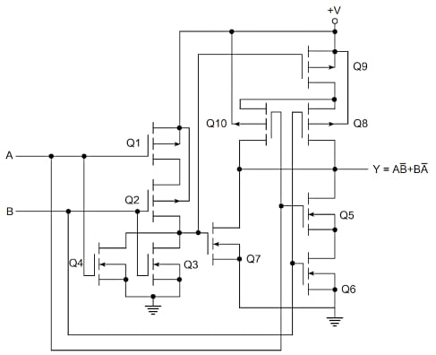
Figure 3. A two-input XOR circuit in CMOS, based on figure 2.
MOSFETs Q1, Q2, Q3, and Q4 form the NOR gate. Q5 and Q6 do the ANDing of A and B, while Q7 performs the ORing of the NOR and AND outputs. Q8, Q9, and Q10 complement the assembly of Q5, Q6, and Q7, inverting the output.
The Exclusive NOR Circuit (XNOR)
Complementing the output of an XOR gate, we get the XNOR gate.
The XNOR function in Boolean notation is
\[Y=AB+\bar{A}\bar{B}\]
Table 2 shows the truth table for an XNOR circuit.
| A | B | Y |
| 0 | 0 | 1 |
| 0 | 1 | 0 |
| 1 | 0 | 0 |
| 1 | 1 | 1 |
Table 2. The truth table for an XNOR circuit.
Since the output is logic 1 for equal inputs, this function is also called the equivalence function.
Figure 4 shows a logic block diagram for the XNOR function
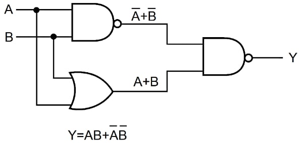
Figure 4. A logic block diagram for the XNOR Gate.
Figure 5 shows an implementation of the arrangement of figure 4 in CMOS
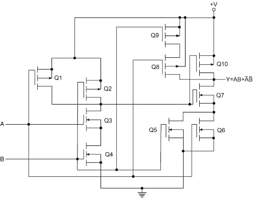
Figure 5. A two-input XNOR circuit in CMOS, based on figure 4.
MOSFETs Q1, Q2, Q3, and Q4 form the NAND gate. Q5 and Q6 do the ORing of A and B, while Q7 performs the ANDing of the NAND and OR outputs. Q8, Q9, and Q10 complement the arrangement of Q5, Q6, and Q7, inverting the output.
The XOR and XNOR operations are widely used functions in adders and parity networks.
The CMOS Transmission Gate Logic
The transmission gate acts like a voltage-controlled switch.
Figure 6 shows the structure of a CMOS transmission gate. It consists of an NMOS in parallel with a PMOS such that complementary voltages control the gates.
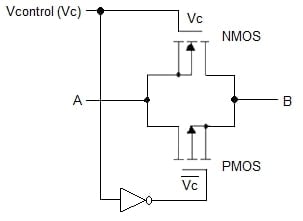
Figure 6. CMOS transmission gate (TG).
Vc = logic 1 biases both NMOS and PMOS into conduction closing the switch and giving an electrical conduction path between A and B (Positive logic).
With Vc = logic 0, both MOSFETs are cut-off, opening the switch and avoiding a direct connection between nodes A and B.
The reason for the parallel combination of an NMOS and a PMOS is simple. An NMOS cannot completely pass a logic 1 voltage, while a PMOS cannot completely pass a logic 0 voltage. Paralleling both transistors allows the transmission of the entire voltage range from 0 V to +V.
Transmission gates are bidirectional, just as a relay’s contacts. From the circuit perspective, this means that the current flow may be in either direction.
Figure 7 shows a common transmission gate logic symbol. A pair of arrowheads placed in opposite directions emphasize the fact that the device is bidirectional. The bubble designates the PMOS gate.
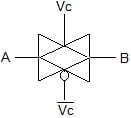
Figure 7. Transmission gate symbol
Transmission gate logic provides an exceptional approach to building helpful switching operations and logic functions, such as multiplexers, XORs, XNORs, flip-flops, and latches
About CMOS implementation of XOR, XNOR, and TG gates
The XOR operation is not a primary logic function. Its output is logic 1 when one and only one input is a logic 1.
The output of an XNOR gate is logic 1 for equal inputs. For this reason, this function is also known as the equivalence function.
The transmission gate operates as a closed switch when Vc = logic 1 and as an open switch when Vc = logic 0, working as a voltage-controlled switch.


The truth table (table 2) for the XNOR circuit is wrong.