 Facebook
 Google
 GitHub
 Linkedin
An introduction to CMOS Technology
Learn about the basic principles of operation of CMOS circuits.
MOSFETs are very common in digital circuits in the form of complementary MOS (CMOS) circuits. CMOS technology fabricates NMOS and PMOS transistors with n- and p-channel MOSFETs paired together on the same chip. It is the leading technology for digital integrated circuits, offering many advantages over using NMOS and PMOS transistors separately.
Introduction
The primary motive for developing the complementary MOSFETs (CMOS) technology was achieving high speed in logic gates for digital circuits, with low power dissipation.
CMOS makes possible the production of numerous potent analog and digital circuit configurations. CMOS is similar to BJT logic devices but switched by voltage rather than current – no current flows into the gate of a CMOS.
Only particular consumer markets used CMOS technology in the 1970s, such as electronic watches. However, in the 1980s, the VLSI technology moved toward CMOS due to advantages such as low power, high noise margin, wider temperature, and voltage operation range, overall circuit simplification, electromigration issue, reliability, and layout ease.
The development of VLSI in the ’80s propelled the integration density to millions of transistors on a single chip. Currently, CMOS is the dominant technology for VLSI digital and mixed-signal designs. CMOS is quicker, better adapted to operate at low supply voltage, and less power-consuming than Transistor-Transistor Logic (TTL).
We´ll see how pairs of n-type and p-type complementary transistors form the basis of the CMOS blocks.
The Inverter
An inverter is a logic element that reverses the applied signal. In digital circuits, binary arithmetic and mathematical manipulation of switching or logic functions are best performed with the symbols 0 (zero) and 1 (one). If the logic levels are 0 for ground or 0 volt, and 1 for V volt, in an inverter, an input level of 0 volt causes an output level of V volt, and vice versa.
Rather than stating these logical operations in words, an alternative method is to give a truth table containing an arrangement of all possible input values and their resultant outputs. For example, table 1 shows the truth table for an inverter.
| INPUT | OUTPUT |
| 0 | 1 |
| 1 | 0 |
Table 1. The truth table for an inverter.
The NMOS Inverter
The common practice uses the gate as an input and the drain as an output, keeping the source and substrate connected to the ground.
Figure 1 shows the symbol and connections for an enhancement-type n-channel MOS (NMOS) with the input grounded. A positive voltage +V supplies power to the drain through a load resistor (RL), biasing the device. The load resistor produces a voltage drop Id ∙RL where Id denotes the drain current. The substrate, source, and gate are grounded.
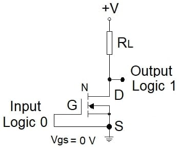
Figure 1. Enhancement-type NMOS inverter with a grounded input.
With the input grounded, there is zero voltage on the gate capacitor – representing logic 0. Thus, the gate capacitor will remain discharged and there will be no channel formed in the transistor. Without a channel present, the transistor operates as an open circuit. It exhibits a high resistance, and hence, the current Id between its drain and source terminals is very low. The output goes positive (+V) – logic 1 – because the voltage drop in the load resistor is negligible.
Then, with a grounded input (logic 0), the transistor is “off,” and the output is very close to the supply voltage (logic 1).
Figure 2 shows the same transistor but with the input connected to the supply voltage +V (logic 1).
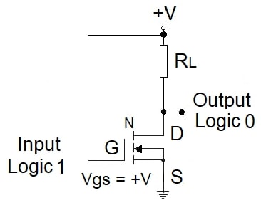
Figure 2. Enhancement-type NMOS inverter with a voltage +V applied to the input.
Now, the gate terminal is connected to a positive voltage. This attracts electrons toward the oxide layer of the gate. As enough charge accumulates below the gate, the result is an excess of electrons, and the silicon turns into an n-type material at the surface.
Now an n-channel connects the n-type source and the n-type drain, reducing the resistance and allowing a drain current Id to flow from drain to source. The positive voltage on the gate turns on the transistor, and it acts as a closed switch. The voltage needed to turn on the transistor is the threshold voltage VT.
When the transistor turns on, it behaves as a resistor. However, as the n-channel has a small resistance compared to the load resistor, the output goes almost to ground – logic 0.
Summarizing, grounding the input (logic 0) makes the output have a voltage very close to the supply voltage(logic 1), and making the input positive (logic 1) results in a grounded output (logic 0), working as an inverter.
The term enhancement-type comes from the fact that the transistor acts as a “normally open” switch and it conducts when it is turned on.
Note that the input is always an open circuit for a DC signal since the gate connects to a capacitor. Therefore, the input current will be non-zero only during the capacitor’s charge/discharge time.
One weak point of NMOS inverters is the need for a continuous current flowing from the power supply to the ground during the ON state of the transistor This can lead to a significant increase in power consumption especially when dealing with a complex circuit.
The PMOS Inverter
The PMOS transistor operates in a complementary fashion, and the inverter circuit connections are the opposite of the NMOS version.
Figure 3 shows the symbol and connections for a PMOS inverter with a voltage +V applied to the input, representing logic 1. The substrate and source are connected to +V and the load resistor to the ground.
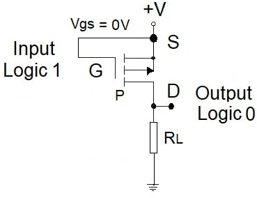
Figure 3. Enhancement-type PMOS inverter with a +V input.
A +V input (Vgs = 0 V) doesn’t charge the gate capacitor keeping the transistor “off.” As a result, the transistor’s resistance is high compared to the load resistor, giving a ground output (logic 0).
Figure 4 shows the PMOS inverter with a grounded input(logic 0 applied to the input).
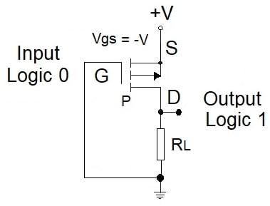
Figure 4. Enhancement-type PMOS inverter with grounded input.
A grounded input (Vgs = -V) charges the gate capacitor, keeping the electrons on the gate side of the capacitor. The charges at the other side of the capacitor are positive, supplied from the positive voltage source.
With enough accumulated positive charges, they convert the n-type silicon’s surface into a p-type material forming a low resistance continuous p-channel between source and drain. This condition turns on the transistor, allowing the drain current Id to flow from the source to the drain.
Since the ON resistance of the transistor is very small compared to the load resistance, its voltage drop is small, and the output is very close to +V(logic 1).
Like the NMOS inverter, logic 0 at the input produces logic 1 at the output and vice versa.
Cross Section of a CMOS
A CMOS is fabricated on a substrate that acts as an electrical reference and gives mechanical support. A cross-section slices the wafer through the middle of the transistor and looks at it on its side.
Figure 5 is a crude cross-section of a CMOS gate where both the NMOS and PMOS transistors are implemented on the same chip. A p-channel is induced on the right and an n-channel on the left for the p- and n-channel devices.
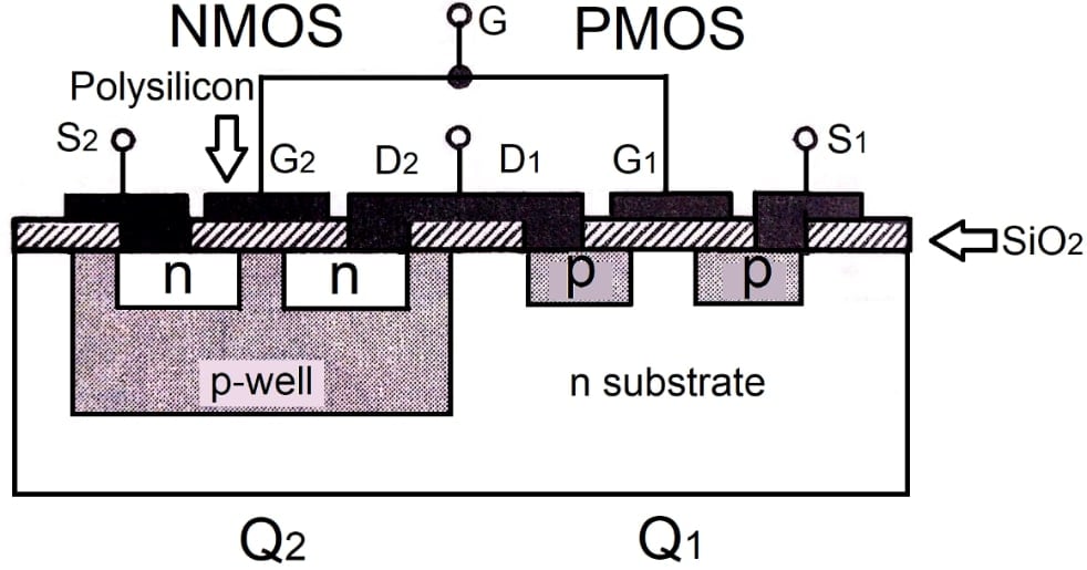
Figure 5. CMOS gate cross-section.
In this arrangement, the PMOS transistor is carried out directly in the n-type substrate (body) and the NMOS transistor in a p-type region commonly referred to as the p-well. A well is a significant, low-doping-level deep diffusion that functions as the substrate for one device and offers isolation between the two device types.
It is also feasible to employ a p-type substrate as a body and form the p-type device in an n-well. The connections made to the n-type body and the p-well are not specified.
The CMOS Inverter
The CMOS inverter is pretty simple, and it reduces the power dissipation to minimal levels. It consists of a pair of enhancement-type NMOS and PMOS, operating as switches, connected in series, as shown in Figure 6. Note that each transistor works as the load resistance of the other transistor.
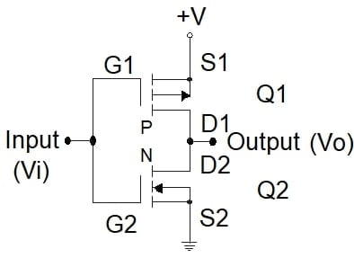
Figure 6. CMOS inverter circuit.
The union of the gate terminals is the input, and the junction of the drain terminals is the output. The PMOS (Q1) substrate and source are bound to +V, whereas in the NMOS (Q2), they are connected to the ground.
Applying +V (logic 1) to the input, Vgs = +V in transistor Q2, it is turned on, and the resistance between its source and drain becomes very small. In contrast, Vgs = 0 V in transistor Q1, keeping it “off” with a high resistance between its drain and source. By computing the output voltage employing the voltage-divider rule, it results in nearly 0 V (logic 0). See figure 7.
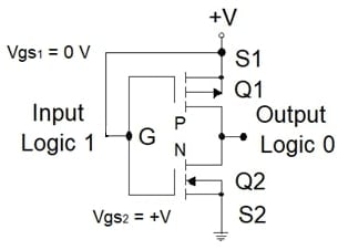
Figure 7. A CMOS inverter with logic 1 at the input.
Therefore, applying +V to the input results in approximately 0 V at the output, establishing the desired inversion process.
Connecting the input to ground, Vgs = 0 V in transistor Q2, keeping it “off,” Vgs = -V in transistor Q1, and it is “on.” Now, Q1 has a low resistance between the source and drain and Q2 a high resistance. Therefore, the output voltage is nearly +V (logic 1) (see Figure 8).
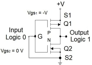
Figure 8. A CMOS inverter with logic 0 at the input.
The NMOS is a pull-down transistor because it pulls the output down to the ground (zero voltage), and the PMOS is a pull-up transistor because it pulls the output up to +V.
Power Dissipation of a CMOS Inverter
CMOS circuits have negligible DC input current. The power dissipated in either state is low because the “off” transistor limits the drain current to the leakage value. The power dissipation is notable only during the input switching.
Although CMOS have low average power requirements, its magnitude depends on the circuit’s activity. For example, in a quiescent circuit – no logical changes occurring – a CMOS consumes minimal power. This feature makes CMOS generally power-efficient compared to TTL. But when changing states at high frequency, the amount of power consumed may increase almost to the level of TTL.
The DC Voltage Transfer Characteristic of the CMOS Inverter
The DC voltage transfer characteristic (VTC) is helpful to quantify the operation of the inverter. However, it is merely an output voltage (Vo) vs. input voltage (Vi) plot.
An inverter employing CMOS technology has a VTC very close to the ideal. For example, figure 9 shows the VTC for a CMOS inverter with Q1 and Q2 matched.
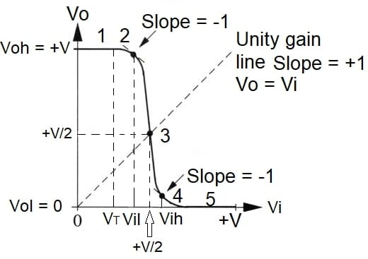
Figure 9. The VTC of the CMOS inverter.
With Q1 and Q2 matched, the inverter has a symmetric transfer characteristic and equal current-driving capability in pull-up and pull-down directions. One significant property of the CMOS inverter is the high output voltage swing.
As shown in figure 9, the VTC has five segments depending on the modes of operation of Q1 and Q2:
Segment 1: Q2 off
Segment 2: Q2 in saturation and Q1 in the ohmic region
Segment 3: Q1 and Q2 in saturation
Segment 4: Q1 in saturation and Q2 in the ohmic region
Segment 5: Q1 off
This plot lets us widen the logic 0 and logic 1 voltage definitions to a voltage range for each logic level. Besides, the limits used to define logic 0 and logic 1 values are different for the output and the input. The significant values are the input voltages Vih and Vil, the output voltages Voh and Vol, and the threshold voltage VT.
Vih and Vil are the VTC points where its slope (dVo/dVi) is −1 V/V. When Vi > Vil, the inverter gain increases, and the VTC enters its transition region. Likewise, when Vi < Vih, the inverter enters the transition region, increasing the gain.
Another essential element of the VTC is the unity gain line. This line has slope = 1 and cuts the curve to a point where Vo = Vi. In this midpoint of the VTC, the inverter switches states. Therefore, with the above VTC, the output changes state precisely midway between ground +V (at +V/2).
The VTC will not be symmetric when transistors Q1 and Q2 are not matched.
Digital designers look for VTC transition regions as narrow as possible, while analog designers focus on the transition region.
A Recap of CMOS Technolgy
Complementary MOS, or CMOS, is ubiquitous in digital circuits, becoming the preferred technology for complex digital integrated circuits.
Complementary means that the transistors operate in pairs, one NMOS and one PMOS in the same chip – both are enhancement MOSFETs.
A turned-on transistor has a low resistance between source and drain. In contrast, the resistance is high when turned off.
A CMOS inverter uses one NMOS transistor and one PMOS transistor connected in series. The PMOS attaches to the power supply +V and the NMOS to the ground.
When the input is logic 0 the NMOS transistor is off, and the PMOS transistor is on. The output is pulled up to logic 1 because it is connected to +V but not to the ground.
With a logic 1 input, the NMOS is on, the PMOS is off, and the output is pulled down to logic 0.
Like any other FET device, a CMOS has insulated input gates. Therefore, the input current is very low.
CMOS designs dissipate a significant quantity of power only when switching occurs, making them more power-efficient than TTL. The feature of not having a static power drain made CMOS a success from its beginnings.


Very good article. I read an article that went into the determination of the S parameters for simulation which was also very good but this one was easier to understand than that one. Of course this one is not as complex but then understandability should not be a function of complexity.