 Facebook
 Google
 GitHub
 Linkedin
Basic CMOS Logic Gates
Learn about gates built with the CMOS digital-logic family.
Logic gates that are the basic building block of digital systems are created by combining a number of n- and p-channel transistors. The most fundamental connections are the NOT gate, the two-input NAND gate, and the two-input NOR gate. This article assumes a positive logic.
The CMOS Inverter or NOT Gate
A NOT gate reverses the input logic state. Figure 1 shows a NOT gate employing two series-connected enhancement-type MOSFETS, one n-channel (NMOS) and one p-channel (PMOS).
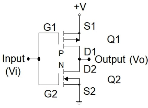
Figure 1. A CMOS NOT gate.
The input is connected to the gate terminal of the two transistors, and the output is connected to both drain terminals.
Applying +V (logic 1) to the input (Vi), transistor Q2 is “on,” and transistor Q1 remains “off.” Under this condition, the output voltage (Vo) is close to 0 V (logic 0).
Connecting the input to ground (Vi = 0 V), transistor Q2 is “off,” and transistor Q1 is “on.” Now, the output voltage is close to +V (logic 1).
Table 1 summarizes these results.
| A | Y |
| 0 | 1 |
| 1 | 0 |
Table 1. The truth table for a NOT circuit.
The CMOS NAND Gate
NAND denotes NOT-AND.
Table 2 shows the truth table for a NAND circuit.
| A | B | Y |
| 0 | 0 | 1 |
| 0 | 1 | 1 |
| 1 | 0 | 1 |
| 1 | 1 | 0 |
Table 2. The truth table for a two-input NAND circuit.
Figure 2 shows a CMOS two-input NAND gate. P-channel transistors Q1 and Q2 are connected in parallel between +V and the output terminal. N-channel transistors Q3 and Q4 are connected in series between the output terminal and ground.
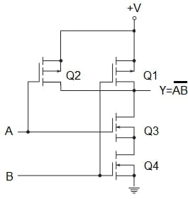
Figure 2. A CMOS two-input NAND gate.
With Q3 and Q4 transistors ”on” and Q1 and Q2 transistors “off,” the output is a logic 0. This condition happens when both inputs, A and B, are logic 1, confirming the lowest row in the above truth table.
With logic 0 in inputs A and B, Q3 and Q4 transistors are “off,” and Q1 and Q2 transistors are “on,” producing a logic 1 output. This is consistent with the first row of the truth table.
When one of the inputs is a logic “1” and the other one is a logic “0”, either Q3 is “off” and Q2 is “on” or Q4 is “off” and Q1 is “on.” The output in both cases is a logic “1,” validating the second and the third rows of the truth table.
The NOR Gate
NOR signifies NOT-OR.
Table 3 shows the truth table for a NOR circuit.
| A | B | Y |
| 0 | 0 | 1 |
| 0 | 1 | 0 |
| 1 | 0 | 0 |
| 1 | 1 | 0 |
Table 3. The truth table for a two-input NOR circuit.
The output of a NOR gate is logic 1 with logic 0 in both inputs. The outcomes for other input combinations are logic 0.
Figure 3 shows a CMOS two-input NOR gate. P-channel transistors Q1 and Q2 are connected in series between +V and the output terminal. N-channel transistors Q3 and Q4 are connected in parallel between the output and ground.
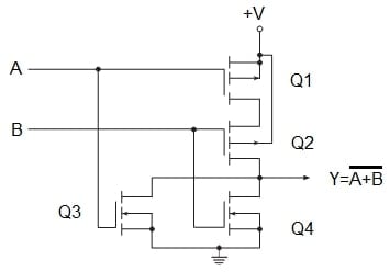
Figure 3. A CMOS two-input NOR gate.
When both inputs, A and B, are logic 0, Q1 and Q2 are “on,” and Q3 and Q4 are “off,” and the output is logic 1. This confirms the first row of the truth table above.
With both inputs logic 1, Q3 and Q4 are “on,” and Q1 and Q2 are “off,” producing a logic 0 output that confirms the last row of the truth table.
For the two remaining input combinations, either Q1 is “off” and Q3 is “on” or Q2 is “off” and is Q4 “on”. In these cases, the output is logic 0 which is consistent with the above truth table.
The AND Gate
We can say that an AND gate is a NOT-NOT-AND or NOT-NAND. Then, it is just a NAND gate followed by an inverter.
Table 4 shows the truth table for an AND circuit.
| A | B | Y |
| 0 | 0 | 0 |
| 0 | 1 | 0 |
| 1 | 0 | 0 |
| 1 | 1 | 1 |
Table 4. The truth table for a two-input CMOS AND circuit.
Figure 4 shows a CMOS two-input AND gate.
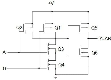
Figure 4. A CMOS two-input AND gate.
The OR Gate
An OR gate is a NOT-NOT-OR or NOT-NOR. Then, it is a NOR gate followed by an inverter.
Table 5 shows the truth table for the OR circuit.
| A | B | Y |
| 0 | 0 | 0 |
| 0 | 1 | 1 |
| 1 | 0 | 1 |
| 1 | 1 | 1 |
Table 5. The truth table for a two-input OR circuit.
Figure 5 shows a CMOS two-input OR gate.
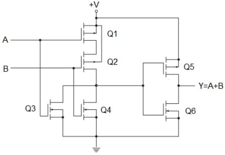
Figure 5. A CMOS two-input OR gate.
The Exclusive OR (XOR) Gate
The output of a two-input XOR circuit assumes the logic 1 state if one and only one input assumes the logic 1 state.
An equivalent logic statement is: ”If B=1 and A=0, or if A=1 and B=0, then Y=1.”
In Boolean notation,
\[Y=\bar{A}B+A\bar{B}\]
Table 6 shows the truth table for a two-input XOR circuit.
| A | B | Y |
| 0 | 0 | 0 |
| 0 | 1 | 1 |
| 1 | 0 | 1 |
| 1 | 1 | 0 |
Table 6. The truth table for a two-input XOR circuit.
Figure 6 shows a two-input logic diagram, and figure 7 shows a CMOS circuit to satisfy the Boolean equation.
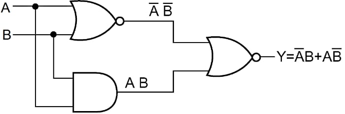
Figure 6. A logic block diagram for the XOR circuit.
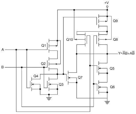
Figure 7. A CMOS two-input XOR gate.
Transistors Q1, Q2, Q3, and Q4 comprise the NOR gate. Transistors Q5 and Q6 make the ANDing of inputs A and B, and transistor Q7 supplies the ORing of the NOR output with the ANDed output. Transistors Q8, Q9, and Q10 complement the arrangement of transistors Q5, Q6, and Q7, inverting the result.
About the Basic CMOS Logic Gates
Combinations of n- and p-channel transistors allow the construction of logic building blocks.
The inverter, NAND, and NOR logic building blocks are the backbone of most digital logic families.
Two primary connections are the two-input NAND gate and the two-input NOR gate.
A NAND gate places two n-channel transistors in series to ground and two p-channel transistors in parallel connected to +V. Only when both inputs are logic 1, the output goes to logic 0.
A NOR gate arranges two n-channel transistors in parallel so that either one can pull the output to ground (logic 0) for a logic 1 (+V) input. It also places two p-channel transistors in series, which must work together to pull the output to logic 1 for logic 0 in both inputs. The output will go to logic 1 only when both A and B are logic 0.
AND and OR gates are NAND and NOR gates followed by an inverter.
An important function that is often needed in logic design is the Exclusive-OR (XOR), with the Boolean expression.
\[Y=\bar{A}B+A\bar{B}\]
The XOR is not a primary gate but constructed by a combination of other logic gates.


The OR gate is missing a junction on the output of the NOR side of the circuit, refer to the NOR schematic for the correction.