Facebook
 Google
 GitHub
 Linkedin
BiAgX HighTemperature LeadFree Pbfree Solder Paste
This article introducest Indium Corporation's BiAgX, a high-temperature lead-free solder paste for surface-mount-technology (SMT) applications.
The world is going lead-free (Pb-free). Over the last 20 years, the use of tin-lead eutectic solders for SMT and similar electronics assembly has been drastically reduced, driven by legislation such as RoHS and RoHS2.
However, high-temperature lead-based solders, especially those with lead (Pb) content >85%w/w, have survived as there remain few alternatives in many applications. This is especially true where the solder joints must survive several low-temperature reflow cycles. For power semiconductor and similar devices, this means discretes or small form-factor modular devices (DrMOS and similar) that are surface-mounted.
Since its formation in 2010, the DA5 consortium (composed of Infineon Technologies, Bosch, STMicroelectronics, NXP Semiconductors and Freescale Semiconductor, Inc.) has evaluated a variety of different alternative technologies and, through the Öko-Institut, concluded that, “based on the information submitted, the use of lead in high-melting point solders in Exemption 8(e) is still unavoidable… The consultants recommend reviewing the exemption by 2021 at the latest.” A summary of the status, as of end of 2014, and appropriate links can be found in reference [1].
HTPbF Solders
So what is the problem with solders? Figure 1 shows some of the wide variety of higher melting solder alloys that are available on the market.
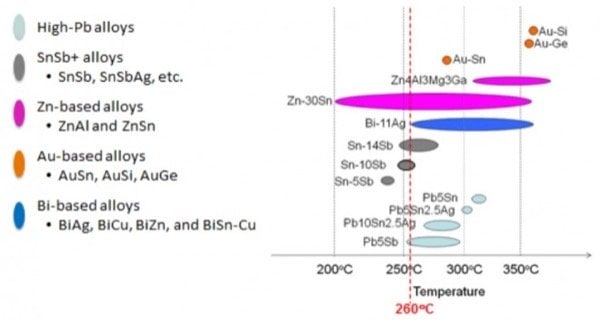
Figure 1: Higher melting solders
Many of these look extremely promising as HTPbF (high-temperature lead-free) solders, as they meet the JEDEC/IPC J-STD-020 requirement for an implicit melting point (solidus) above 260°C (or 265°C, depending on your interpretation of the standard). However, each solder has a fundamental flaw or flaws, that makes it difficult to implement as a die-attach material:
- Antimony (Sb)-based solders are not acceptable to some customers, and do not quite meet the reflow temperature requirements
- Zinc (Zn)-based solders oxidize readily, making void-free reflow difficult to implement without severe process constraints
- Gold (Au)-based alloys are expensive and, due to both their cost and their high tensile strength, are limited to small die only
- Bismuth (Bi)-silver [2] does not form an intermetallic with standard metallizations, and, therefore, does not solder well
Alternative Joining Technologies
Several alternative technologies are emerging as Pb-free replacements, the most promising being nanosilver sintering materials. Sintered silver and similar technologies, such as transient liquid phase materials, may well meet the die-attach needs of high-current density and higher Tj devices into the future [3]. They also necessitate significantly increased materials costs, new capital equipment costs, increased sensitivity to the condition of underlying metal surfaces (such as oxide and roughness), and lower production rates (UPH) over conventional solder-based processes [4]. This makes these materials unsuited for use in smaller, cost-sensitive discrete devices and power modules.
For this reason, a “drop-in” HTPbF solder-based solution is an ideal material. Of all the form factors of die-attach solder – solder paste, fluxless wire and engineered solders (solder preforms) – solder paste has the most flexibility as it can be used on die from under 1x1 mm (where specific alloy types eliminate skewing and tilt) to 10x10 mm or higher, with vacuum reflow.
BiAgX® Solder Paste
Bismuth-silver (BiAg11) clearly meets the criterion of a solidus >260°C. However, it does not solder in any useful, mechanically-strong, way to standard die and leadframe/DBC metallizations. Yet, it has been found that by adopting a mixed alloy approach [5], it is possible to significantly enhance the solderability – even onto challenging surfaces such as alloy 42 (Figure 2). Die-attach to common leadframe surfaces, such as “bare” (or organically-treated) copper, silver spot-plate, and common die surface finishes including Ti ENIG, ENEPIG and NiAg, is therefore feasible using this approach.
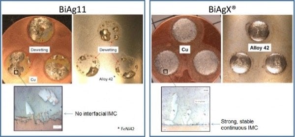
Figure 2: Comparison of BiAg11 and BiAgX®
For this reason, this unique alloy-design approach was taken to begin to develop an HTPbF solder paste material with the key characteristics of:
- Drop-in alternative to standard solder paste (deposit, reflow, and cleaning) processes without capital expenditure
- Printable and dispensable versions, just like any other solder paste
- No pressure needed on die and no extraneous process steps
- Solderable to standard die and leadframe/DBC metallizations, including NiAu, NiAg and Cu and CuAg, to meet widely-accepted industry standards of <5% single and <10% total voiding
- Solidus of final joint >260°C
- Reliability of final joint
- Fluxes that are washable with standard cleaning chemistries
- Cost parity with standard solder materials (no gold, indium or specialty materials such as nano particulates)
BiAgX® Metallurgy
The basis of the BiAgX® solder paste technology is the use of two or more different solder alloys in combination. An outline of the technology is shown in Figure 3. During reflow (A), a tin-based, lower-melting alloy melts first (B), dissolving any sacrificial protective metals (such as gold or silver) and soldering to copper and nickel through the free energy of formation of intermetallics. As the temperature rises further, the second, higher-melting phase begins to melt, at its own solidus temperature. As it melts, the high-melting alloy dissolves into the (now molten) lower-melting liquid phase. Heating continues until the liquidus of the higher melting phase is reached and all the solder is molten (C). If voiding is sufficiently low, the joint can now be allowed to cool down.
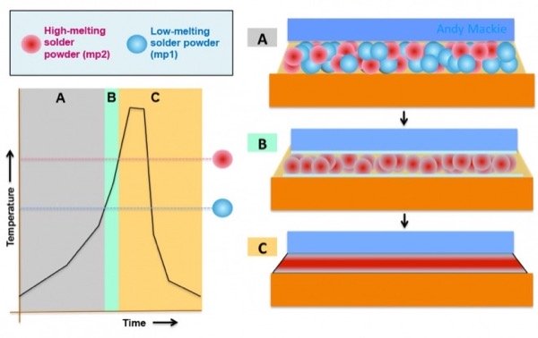
Figure 3: Basis of BiAgX® solder paste technology
By an appropriate choice of alloy in the appropriate ratio, the low-melting phase that is necessary for the functioning of the BiAgX® can be completely consumed by reaction to intermetallics during reflow, preventing remelt below the standard 260°C limit for J-STD-020 preconditioning.
Reliability
Low solder joint voiding is key to the functioning (characterized by RDSon and, more critically, RthJC) and reliability of the finished device. Voiding is a function of several factors, including flux formulation, powder oxidation, and surface metallization. This can be controlled well within standard needs for smaller module and discrete devices [6].

Figure 4: Die shear strength of 2x2 mm SiC die on DBC substrates as a function of aging time at 200°C
The reliability of BiAgX® joints has been studied under high-temperature storage (200°C) [6] (data shown in Figure 4) and JEDEC thermal cycling and thermal shock conditions and been shown to be significantly improved over standard high-Pb solders [7].
Conclusion
The mixed alloy solder paste approach is showing wide acceptance among customers in the target market of discrete and small power module power management devices, especially by those located in Asia.
The technique also shows much broader applicability in some MEMS and SMT applications requiring a higher temperature Pb and Sb-free solder. A family of solder paste materials based around this technology [5] is under development to meet specific customer needs.
About the Authors
Andy C. Mackie works at Indium Corporation as the Senior Product Manager since July 2012 where he has driven enhanced profitability by bringing novel materials into new and emerging markets by engaging with key customers and equipment suppliers to expand understanding of processes and speed customer time to market. He earned his Bachelor's Degree in Chemistry at the University of Leicester. He also holds a Master's Degree in Colloid and Interface Science and Ph.D. in Physical Chemistry earned from the University of Bristol and University of Nottingham respectively.
Hongwen Zhang works as the Research Metallurgist at Indium Corporation since May 2018 where he is focused on Drop-In High-Temperature Lead-Free Solders. He is experienced in Pb-free solders and semiconductor packaging process, semiconductor package failure analysis, metal matrix composite design and manufacturing, and more. He holds a Master's Degree in Materials Science and Engineering at the Institute of Metal Research, Chinese Academy of Sciences. He also holds a Degree in Mechanical Engineering and Ph.D. in Materials Science and Engineering both earned from Michigan Technological University.
References
- http://www.indium.com/blog/elv-2014-high-lead-pb-in-automotiveelectronic....
- Lalena et al. “Experimental Investigation of Ge-Doped Bi-11Ag as a New Pb-Free Solder Alloy for Power Die Attachment” Journal of Electronics Materials, 31(11), 2002, pp. 1244-1249.
- Russo et al. “Reliability of new Pb free die attach materials for power devices,” Proceedings of Automotive Electronics Council Reliability Workshop 2014, Novi, MI.
- Siow, “Are sintered silver joints ready for use as interconnect materials in microelectronic packaging?” Journal of Electronic Materials, 43/4, 2014 pp. 947-961.
- US Patent 9,017,446.
- Johnson et al. “Lead-free Solder Attach for 200°C Applications,“ Proceedings of iMAPS HiTen Conference, Oxford, UK, 2013.
- Zhang et al. “Reliability of Lead-Free BiAgX Pastes for High Temperature Die-Attach Application,” Proceedings of TMS Conference, San Antonio, TX, 2013.