Facebook
 Google
 GitHub
 Linkedin
Achieving Increased Solder Joint Reliability and Low Voiding in High Power Applications
This article features Indium Corporation reinforced solder preforms that improve the reliability of solder joints with consistent solder joint bondline.
Solder joints in higher power applications are being challenged like never before. In addition to providing mechanical and electrical interconnections between components and boards, solder joints must also dissipate significant amounts of heat (Figure 1).
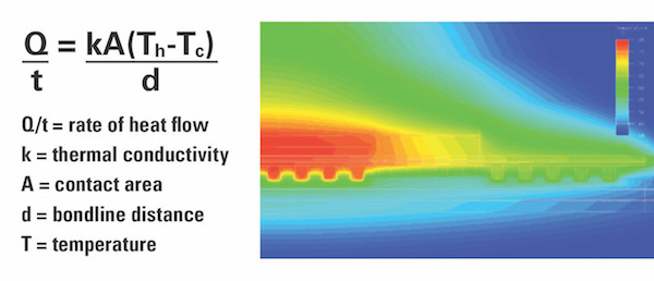
Figure 1. Factors influencing heat flow.
At a relatively low melting point, the solder can bond two surfaces that have a much higher melting point, such as copper. In addition, the bond has very high electrical conductivity and thermal conductivity. Relative to thermal conductivity, SAC solder is about 35W/mK. In comparison, thermal greases are often in the 1–5W/mK range.
Therefore, the solder is much more capable of dissipating the heat generated by the power device or power electronics device. The contact area is another factor in which solder performs well—it is ideal when forming an intermetallic bond at the interfaces.
Recognizing the Problem
The areas that can potentially hinder the thermal performance of a solder joint are bondline distance and voiding within the solder joint itself. Because the soldering process involves the metal becoming molten, the component will float on the molten solder due to the surface tension.
Unfortunately, when a component floats on molten metal, the component may not remain parallel upon solidification. This lack of parallelism can result in hot spots. Additionally, this lack of control can mean variability in thermal performance from device to device.
The other area that negatively impacts thermal performance is voiding within the solder joint. Even though the solder itself transfers heat very well, large voids will act as an insulator and significantly slow that thermal transfer.
The Solution
To address the challenges facing solder joints in high power applications, a reinforced solder preform was developed (Figure 2). This technology takes a solder preform and embeds a high-melting-point metal standoff into it. The solder can be virtually any alloy currently used in electronics; the SAC305 is very common.
The standoff is a precise thickness which is based on the final solder joint bondline that is being targeted. These preforms can be flux-coated if needed for the application.
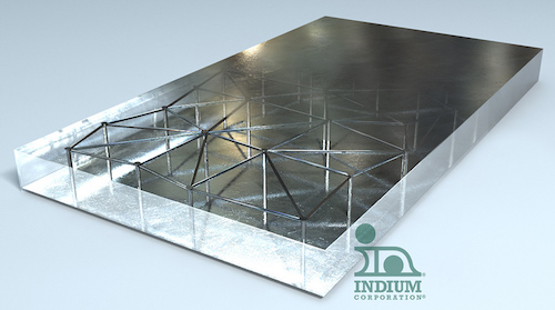
Figure 2. InFORMS® is a reinforced matrix solder preform.
During reflow, the solder will melt and form the intermetallic bond with the component and board. The component will collapse during reflow. Since the standoff material can be made of a metal that has a much higher melting point than the solder, it does not melt.
Therefore, the collapse of the component will be limited to the thickness of that standoff. Because this is manufactured to a precise thickness and is uniform across the entire solder area, the final bondline will be consistent.
Proven Bondline Consistency
In work done by Booth, et al. [1], a reinforced solder preform was used in an IGBT assembly to bond the DBC to the baseplate. In this study, a 95Sn/5Sb preform was embedded with a standoff having a thickness of 0.008”. The assembly process, like most IGBTs, was done in a fluxless, vacuum reflow process. After reflow, they looked at overall device planarity, as well as thermal cycling reliability.
Figure 3 shows laser profilometers of an IGBT assembled with a reinforced solder preform next to one assembled with just a standard solder preform. When assembled using the preform with the built-in standoff, the overall co-planarity was better with a mean deviation of 52.5 micron versus 67.5 microns with a standard preform. The maximum deflection for the reinforced solder preform was 60 microns, while the standard preform had a maximum deflection of 90 microns.
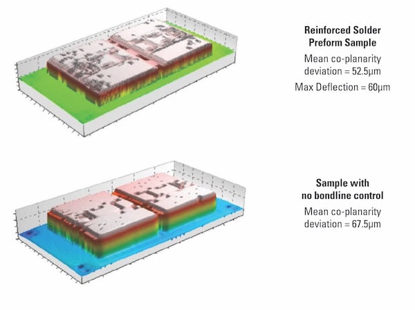
Figure 3. Reinforced solder preform results in solder joints that have a much more consistent bondline.
Clearly, the Booth, et al. work shows that the reinforced solder preform results in solder joints that have a much more consistent bondline. Additionally, they ran thermal cycling from -50 to +150°C with one-hour dwells. The C-SAM images shown in Figure 4 compare a standard solder after 600 cycles to a reinforced solder preform after 800 cycles.
The standard solder is showing delamination, which is believed to be a result of an inconsistent bondline thickness. Even after 200 additional cycles, the reinforced solder joint shows no delamination. This provides sufficient evidence that the bondline consistency has an impact on overall solder joint reliability.
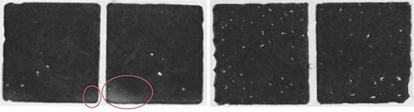
Figure 4. The image on the left is a standard preform showing solder joint delamination after 600 cycles. The image on the right is a solder joint formed with a reinforced solder that shows no delamination after 800 cycles.
New Proof of Low-Voiding
The earlier work done shows that reinforcing the solder preform will result in solder joints with a more consistent and reliable bondline. However, voiding is another important factor when soldering. With so many possible variables when designing reinforced preforms, it was previously unclear how these variables would impact voiding.
Therefore, a test coupon and DOE were developed to evaluate the following variables:
- The substrates tested were 0.354” x 1.26” and plated with immersion Sn.
- Sandwiched between these substrates was a SAC305 reinforced preform.
- Five grams of pressure were applied to the coupons to force collapse of the solder during reflow.
- The reflow profile was linear at about 1°C/sec with a peak temperature of around 245°C using an air reflow process.
- This experiment looked at 0.010”, 0.012”, and 0.016” total preform thicknesses.
- Two flux percentages of 1% and 2% were examined.
- For each leg, 25 coupons were reflowed.
When analyzing the voiding data from the DOE, there were some clearly identifiable differences among the reinforced solder preform designs. The summary of the data is shown in Figure 5. For the standoff type, the first two characters (LM or SM) refer to the amount of spacing. The LM is much less densely packed with standoff metal.
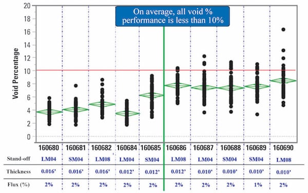
Figure 5. Summary of voiding results.
The SM has about 3x the packing density, which means much more standoff metal was embedded into the preform of equal size.
The second two characters refer to the amount of standoff (04 is 0.004” and 08 is 0.008”). All designs exhibited an average void percentage of less than 10%. Five of the designs did not have any data points over the 10% mark. Further analysis was done to determine the significance of specific attributes.
In this statistical analysis, if the P-value is less than 0.05, the mean of at least one of the factors is statistically different.
Preform Thickness
LM04, LM08, and SM04 data sets were analyzed separately for the impact of overall preform thickness. In every case, a higher overall preform thickness resulted in less voiding. Voids escape out of molten solder due to the surface tension by forcing them to the perimeter.
Unmelted metal in the molten solder could impede the pathway for these voids to escape. By having more solder available, the voids can possibly escape around the metal matrix prior to the complete collapse of the solder joint.
Packing Density
When exploring the packing density of the standoff material, the void differences between SM and LM were examined individually for each overall preform thickness. The results here are not as clear. For the 0.016”- and 0.010”-thick preforms, the packing density did not significantly impact the void performance. For the 0.012” thickness, the SM product was statistically better than LM.
Based on these results, it cannot be conclusively stated that packing density does or does not influence voiding. The data suggests that at most this factor would only be a very minor contributor to voiding.
Standoff Thickness
In this case, LM04 was compared to LM08 for each of the preform thicknesses. For every preform thickness, the higher standoff (08) always resulted in statistically significant higher voiding. This also can be explained relative to the solid standoff material impeding the escape of the voids.
Because the 08 material is thicker, there would be a higher overall volume of standoff metal embedded into the preform versus the 04 material. More solid material has the potential to impede the ability of the void to escape the molten solder.
Flux Percentage
Based on the chemistry of oxide removal and volatilization, it is expected that more flux will result in more voiding. Basically, as the product is going through reflow, the flux is removing oxides on the metal surfaces. That oxide removal process creates some vapor.
Additionally, there are non-active ingredients in the flux that will also volatilize at elevated temperatures. Both of these attributes of fluxes could result in vapor getting entrapped in the molten solder. However, the work in this study did not show any significant difference between 1% and 2% flux.
It can only be speculated that perhaps the 1% difference in flux was not enough to impact the voiding. This is an area where further work could be done.
Summary of Solder Joint Bondline Study Results
It is known from previous works that reinforced solder preforms can help to improve the reliability of solder joints by providing a consistent solder joint bondline. The new data obtained from the more recent study shows that the final thickness of the preform, the packing density of the standoff material, and the thickness of the standoff all can be adjusted to impact the amount of voiding in the solder joint.
Through an optimized design of the reinforced preform, it is clear that this technology can produce high-reliability, low-voiding solder joints without incurring additional process steps such as wire bond stitching to control the collapse of the solder.
About the Authors
Tim Jensen is the Senior Product Manager for Indium Corporation’s Engineered Solder Materials and has been with the company since 1997. He has a bachelor’s degree in chemical engineering from Clarkson University and a master’s degree from Syracuse University.
Sunny Neoh is the Assistant Product Manager for Engineered Solder Materials in Asia. Sunny has more than 12 years of engineering experience, with a special emphasis on process improvement in the SMT industry. He earned his bachelor’s degree in Material Engineering from the Universiti Sains Malaysia and is certified as a Six Sigma Green Belt.
Adam Murling is a technical support engineer based at Indium Corporation’s global headquarters in Clinton, N.Y., USA. He is an SMTA-Certified Process Engineer, an active blogger, and he has authored technical papers on wave solder fluxes and solder preforms. Murling has a bachelor’s degree in chemical engineering from Clarkson University.
Seth Homer is a Product Manager for Indium Corporation’s Engineered Solder Materials. He has worked with Indium Corporation for over 20 years, serving in both manufacturing operations and marketing roles. Currently, Seth is working with the IGBT and power electronics industries, gaining insight by traveling to customer sites globally and working closely with manufacturing internally as he helps support current production demand and future product development.
References
- J. Booth, et al. “Novel Technique to Reduce Substrate Tilt and Improve Bondline Control between AlN Substrate and AlSiC Baseplate in IGBT Modules,” PCIM 2016. This data was first presented at SMTA Pan Pacific Microelectronics Symposium, February 6-9, 2017, Kauai, Hawaii, USA.
This article originally appeared in the Bodo’s Power Systems magazine.