Facebook
 Google
 GitHub
 Linkedin
Comparing Thermal Performance of Die-Attach Materials
Silver sintering and transient liquid phase soldering are replacement technologies for bonding using high reliability solder alloys. This article compares the thermal impedance of die-attach materials, including those obtained using silver sintering, to gain insight into their thermal performance.
Transient liquid phase soldering (TLPS) technology is considered as an alternative to soldering using high-reliability solder alloys (e.g., Sb-containing solders, AuSn20, etc.). The end-of-life and mechanical characteristics of such bonds based on the Sn-Cu system exhibit behaviors comparable to those obtained using the silver sintering die-attach technology [1,2].
At first glance, the obvious drawback of TLPS joint might be the low thermal conductivity compared to that of sintered silver caused by the low thermal conductivity of Sn-Cu intermetallics. Literature data regarding the thermal properties of TLPS materials are scarce, especially in a layered form. Given the recent promising results of reliability studies on the die bonds obtained using our preform-based diffusion solder material PFDS400 [3], the results of thermal resistance analysis may complement the overall picture of its capabilities as a die-attach material. In order to gain an idea about the thermal performance of the latter, a thermal impedance comparative study of different bond materials was performed. This inspection method, well-known in power electronics, provides inferences on the thermal resistance of layers beneath the power semiconductor element of a power module stack. In this study, we obtained and compared Zth-characteristics for joints bonded using different types of PFDS400 with those bonded using conventional solders and silver sintering.
Material Description and Sample
For the Zth-measurements, six types of assemblies were manufactured using power diodes (SEMIKRON CAL-DIODE SKCD 61 C 170 I HD) in the dimension of 7.8 mm x 7.8 mm and two different substrates. The first type was bare copper DCB consisting of Cu/ Al2O3/Cu layers with thicknesses of 300 µm/ 380 µm/ 300 µm, respectively. The second type was an Ag-thick-film substrate (Fraunhofer IKTS Systemintegration und AVT) with layers Ag/Al2O3 of 9 µm and 380µm thickness, respectively. The diode backside metallization consisted of Ni/Ag layers. The front side metallization consisted of a bondable Al layer. The overall die thickness was 304 µm. The following die-attach materials were used: solder preforms of SnAg3.5 and SnAg3.0Cu0.5, a family of preform-based diffusion solders PFDS400 M, and silver paste (for silver sintering). Solder preforms of SnAg3.5 and SnAg3.0Cu0.5 alloys were modified using integrated spacer wires in order to guarantee a homogeneous bond line thickness comparable to the other joints. This type of preform belongs to the family WireGuard preforms designed by Pfarr Stanztechnick GmbH. The reflow soldering and TLPS bonding of semiconductors was performed by PINK GmbH Thermosysteme using their VADU vacuum reflow soldering system. The silver sintering was performed by PINK GmbH Thermosysteme using a SIN sintering system. Scanning acoustic microscopy (С-SAM) was used to examine the joints for void formation. For the Zth-measurement, 7 samples of each material configuration were built up. After the Zth-measurements, microstructures of each connection type were studied using cross-sectional analysis. The die-attach material and the substrate type used are presented in Table 1.
Table 1. Compared test vehicles, consisting of the die attachment material, its layer thickness, and the substrate type used.
| Die attachement material | Type | Thickness [µm] | Substrate Type |
| SnAg3.5 - WireGuard® | Preform with integrated spacer wires | 50 | Bare Cu-DCB |
| SnAg3.0Cu0.5 - WireGuard® | Preform with integrated spacer wires | 50 | Bare Cu-DCB |
| PFDS400®M/Cu | TLPS preform, Cu-Sn-System | 50 | Bare Cu-DCB |
| PFDS400®M/Ni-Cu | TLPS preform, Cu-Ni-Sn-System | 50 | Bare Cu-DCB |
| Silver Sinter Paste | Paste (Externally supplied material) | 20-25 | Bare Cu-DCB |
| PFDS400®M/Ag | TLPS preform, Ag-Sn System | 30 | Ag Thickfilm Substrate |
| Silver Sinter Paste | Paste (Externally supplied material) | 20-25 | Ag Thickfilm Substrate |
Joint Quality and Material Characterization
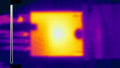
The C-SAM images shown in Figure 1 demonstrate a high quality for all joints manufactured for this study, exhibiting a low degree of void formation.
The two contrasting strips visible in Figure 1a correspond to the location of the spacer wires of SnAg3.5 and SnAg3Cu0.5 solder preforms.
Figure 2 shows cross-sectional images corresponding to the joints shown in Figure 1. The microstructures confirm the high joint quality demonstrating a dense structure with a low degree of microporosity in both silver-sintered and TLPS joints as well as in conventional solder joints. The TLPS joints are characterized by the formation of a number of Sn-containing intermetallic compounds providing their high-temperature mechanical stability. Depending on the assembled parts and their metallization, the following intermetallics were formed: Cu6Sn5, Cu3Sn, Ag3Sn, and Ni3Sn4. The formation of intermetallics was also observed in the SnAg3.5 and SnAg3Cu0.5 joints at the location of the Cu wire spacer (Figure 2a). Based on the cross-sectional analysis, the total joint thickness was determined and summarized in Table 1 together with supplementary information.

Figure 1. C-SAM images of the die-attach joints (material-substrate): a) SnAg3.5 or SnAg3Cu0.5 WireGuard® preforms - DCB; b) PFDS400®M/Cu - DCB; c) PFDS400®M/Ni-Cu - DCB; d) sintered Ag - DCB; e) sintered silver - Ag-thick-film substrate; f) PFDS400®M/Ag - Ag-thick-film substrate. Image used courtesy of Bodo’s Power Systems [PDF]

Figure 2. Cross-sectional images of the die-attach joints (material substrate): a) SnAg3.5 or SnAg3Cu0.5 WireGuard® preforms - DCB; b) PFDS400®M/Cu - DCB; c) PFDS400®M/Ni-Cu - DCB; d) sintered silver - DCB; e) sintered silver - Ag-thick-film substrate; f) PFDS400®M/Ag - Agthick-film substrate. Image used courtesy of Bodo’s Power Systems [PDF]
Measurement Procedure
The measurement of the thermal impedance Zth of power electronic devices is based on the heat flow between the source of the dissipated power (e.g., a power chip) and a reference point. This reference point can be set at the underside of the device (case), at the heat sink, or at the ambient temperature, respectively. During the measurement procedure, the device is heated up by the implementation of a constant load current for a specific on-time. At the end of the heating phase, the power loss is determined by measuring the voltage drop and load current. When the current is switched off, the measurement of Tj and Tref is started and tracked until a constant temperature is reached. The temperature-dependent voltage drop of the pn junction of the chip is used as a temperature-sensitive electrical parameter (TSEP) by introducing a sufficiently small measurement current into the device to prevent self-heating.
For the calculation of the thermal impedance, equation (1) is used:
\[Z_{th}(t)=\frac{Tj(t)-T_{ref}(t)}{P_{V}}\,\,\,(1)\]
To obtain the desired Zth function, the cooling curve (Zth,down) must be converted into a heating curve (Zth,up). By use of equation (2) with Rth estimated at the time point with the highest measured temperature, this conversion is completed.
\[Z_{th,up}(t)=R_{th}-Z_{th,down}\,\,\,(2)\]
With the help of thermal simulations, the time constants of the different layers can be estimated. With this knowledge, an evaluation of the thermal impedance of the solder or sinter layer, respectively, is performed at about 5-15 ms.
Results and Discussion
Using the measurement procedure described above, Zth functions were obtained for die-bonding with DCB-substrates (Figure 3) and with Ag thick film (Figure 4).

a)

(b)
Figure 3. a) Zth curves of the die-attach joints with DCB b) Zth functions of the die-attach joints with DCB on a timescale in the vicinity of 7ms. Image used courtesy of Bodo’s Power Systems [PDF]

Figure 4. Zth-curves of the die-attach joints with Ag-thick-film. Image used courtesy of Bodo’s Power Systems [PDF]
For a close comparison of the Zth functions of the die-attach joints with DCB shown in Figure 3b, a smaller area around the 7 ms time constant was considered, where the influence of the bonding material was assumed. The Zth values detected at 7 ms are summarized in Table 2.
Table 2. Zth values for the die bonding with DCB-substrates measured at 7ms
| Material | Zth-value around 7 ms [K/W] |
| SnAg3.5 WireGuard | 0,0993 |
| SnAg3Cu0.5 WireGuard | 0,0948 |
| PFDS400 M/Cu-Ni | 0,0921 |
| PFDS400 M/Cu | 0,0879 |
| Silver Sintering | 0,0865 |
Comparison of the Zth functions reveals very little difference (0.0014 K/W at 7 ms) between those of the 25 µm thick silver sintered joints and those of the 50 µm thick PFDS400 M/Cu diffusion soldered joints on the Cu-DCB carrier. At the same time, no noticeable difference in Zth values was observed between 30 µm thick PFDS400 M/Ag and a 25 µm thick silver sintered connection on the Ag-thick-film substrate. The SnAg3.5 and SnAg3Cu0.5 WireGuard preforms show higher Zth values demonstrating elevated thermal resistivity compared to other bond materials, which is expected for tin-based solders. The PFDS400 M/Ni-Cu material exhibits reduced thermal performance compared to the copper-containing PFDS400 variant, as it contains more of the less thermally conductive Ni compared to highly conductive Cu. Nevertheless, PFDS400 M/Ni-Cu exhibits lower thermal impedance compared to SnAg3.5 and SnAg3Cu0.5 WireGuard preforms. Despite the multi-layered structure of PFDS400 preforms and thus the presence of numerous thermoresistant boundaries, this material demonstrates a thermal performance comparable to Ag-sintered joints. This is regardless of the fact that the Ag-sintered joints shown in Figure 1 d, e, and Figure 2 d, e exhibit fairly good sintered structures with a minimal degree of porosity. Although the joints with PFDS400 M/Cu and PFDS400 M/Ag are almost twice as thick as Ag-sintered joints, they exhibit comparable thermal resistance.
Takeaways of Thermal Impedance Measurements of Die-Attach Materials
In this article, a comparative analysis of thermal impedance measurements of different die-attach materials was performed. The results have shown that despite the layered structure and thicker joint gap, the PFDS400 material, namely the PFDS400 M/Cu and PFDS400 M/Ag variants exhibited values comparable to silver-sintered joints. PFDS400 M/Cu-Ni exhibited higher thermal resistivity due to the reduced thermal conductivity of the Ni layer, albeit lower compared to SnAg3.5 and SnAg3Cu0.5 solders. Given that the reliability of semiconductor solder joints with PFDS400 is as good as that of sintered silver, the results of this work indicate that this material offers a better alternative to high-reliability, lead-free solders and competes head-to-head with silver sintering technology.
References
[1] A. Otto et al., “Evaluation of Ag-sinter and CuSn-TLP based joining technologies on lead frame,” PCIM Europe 2018, Nuremberg, Germany
[2] K. Guth et al., ”End-of-life investigation on the .XT interconnect technology” PCIM Europe 2015, Nuremberg, Germany
[3] B. Ottinger et al., “Reliability of lead-free solders for die attach in automotive power modules,” 2022 IEEE 24th Electronics Packaging Technology Conference, Singapore, Singapore.
Acknowledgment
We would like to thank the Power Electronics Group of Chemnitz University of Technology for conducting the Zth measurements and for their support in the interpretation of the results. We would also like to thank the Systems Integration and Electronic Packaging Group of Fraunhofer IKTS and the company Pink GmbH Thermosysteme for providing materials, carrying out the joining processes, and inspection of the samples.
This article originally appeared in Bodo’s Power Systems [PDF] magazine and is co-authored by Dmytro Pavlyuchkov and Ralph Mädler of Pfarr Stanztechnik GmbH.
Featured image used courtesy of Adobe Stock