Facebook
 Google
 GitHub
 Linkedin
4th Generation Field Stop IGBT with Enhanced Latch up Immunity
This article highlights Fairchild Semiconductor 4th generation Field Stop (FS) IGBT that offers superior device performance under static and dynamic states.
Thanks to their low conduction and switching energy loss, IGBTs are widely used in high power applications such as power supplies, motor driving inverters, electrical vehicles, etc.
The requirement for more state of the art power devices for power applications has triggered efforts around novel silicon based development, as well as wide band gap material development, to achieve characteristics that stretch the ideal limit of silicon. The theoretical silicon limit for IGBTs was investigated by A. Nakagawa, [1] and in order to realize optimal silicon characteristics, various injection methods to enhance IGBT structures were proposed, such as CSTBT, IEGT, and narrow mesa IGBT [2-4].
High electron injection efficiency from the MOS gate is required
In order to push IGBT silicon to the limit, extremely high electron injection efficiency from the MOS gate is required, while the hole carrier injection should be restricted to the level of contribution only for the conductivity modulation. [1] For Fairchild’s 4th generation FS IGBTs, electron injection was enhanced by a very fine cell pitch design and hole carrier injection was restricted by a new buffer structure, achieving remarkably better trade off performance as well as strong latch up immunity. To realize the narrow mesa or high-density cathode design of the trench IGBT, a self-aligned contact process was applied.
This proved to be very effective in optimizing the critical dimension of active cell design for the enhanced ON-state performance, as well as to maximize the latch up current capability. In addition, multiple buffer layers were adopted for the anode side of the IGBT in order to not only effectively control the minority carrier injection during the on state, but also to completely block the electric field during the off state [5].
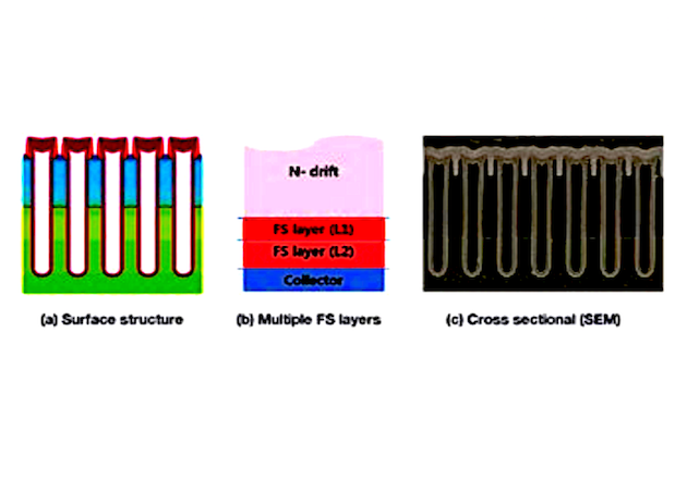
Figure 1: Proposed structure
Vertical structures of the proposed IGBT
The vertical structures of the proposed IGBT are illustrated in Figure 1 for the cathode and anode side. Figures 1(a) and 1(c) show that the high density cell design with submicron narrow mesa width is successfully realized by employing a self-aligned contact process, without any photo misalignment. The higher density active pattern shown in this figure is beneficial for extremely enhanced electron injection from the cathode side and, as a result, the higher electron current density.
The new buffer structure with multiple layers, as shown in Figure 1(b), is very helpful for the ideal carrier distribution during IGBT operation. Generally, a single buffer layer with 1~5e15cm–3 is used for both hole injection control and electric field blocking efficiently. In this experiment, a thin buffer layer with a much higher doping concentration was additionally embedded for better trade-off performance.
In other words, the higher doping concentration in the double buffer layer is even more effective for the electric field blocking and hole carrier injection control by the first FS layer (L1). The lower doping concentration for the second buffer layer (L2) is preferred for forming a lightly doped p-type collector for high-speed switching performance without any lifetime killing process. In addition, the device switching waveform can be effectively improved by varying the doping concentration and thickness of the double buffer layers, due to proper carrier distribution control during switching ON/OFF operation.
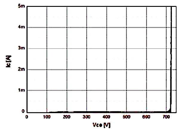
Figure 2: Measured breakdown voltage
As is illustrated in Figure 2, the measured static breakdown voltage is about 720V with hard waveform. It means that the double buffer layer is sufficiently blocking the electric field in the off state. In this work, 650V-50A-rated 4th generation FS IGBT was developed and evaluated. The trade-off performance was also compared with the 3rd generation FS IGBT, as shown in Figure 3, under a current density of 470A/cm2 for ON-state voltage drop and turn-OFF hard switching. The proposed 4th generation FS IGBT shows better trade-off performance, compared with previous generation IGBT technology. (About 30% turn-OFF energy loss (Eoff) reduction at the same on-state voltage)

Figure 3: Trade-off performance comparison
Latch up immunity
The latch up immunity is evaluated under static and dynamic conditions, as shown in Figures 4 and 5 respectively. Figure 4 shows that the maximum static saturation current is around 4000A/cm2 with no latch up phenomenon.
Dynamic latch up characteristics
In particular, for the dynamic latch up characteristics shown in Figure 5, the proposed FS IGBT shows a very strong ruggedness and also safely operates over 3000A/cm2 current density without failure under the severe hard switching condition (T=150C, Rg=0ohm, Vge=+-15V to induce very high voltage slop (dv/ dt) between collector and emitter). This is because the self-aligned process removes possible local weak points from the contact photo misalignment so that the injected minority carrier can evenly flow without crowding into any specific area.
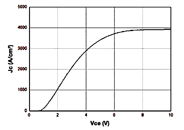
Figure 4: Static latch up characteristics
Summary
4th generation FS IGBT technology was successfully developed based on the injection enhanced carrier profile that was optimized with an effort to approach the limits of IGBT silicon. This new generation of FS IGBTs with a high-density cell structure and well-designed double buffer layer shows superior device performance under static and dynamic states as well as strong latch up ruggedness. We’ve confirmed that the self-aligned process is a very effective method for the embodiment of submicron trench and mesa active design, as well as for realizing strong latch up immunity. For the following generation of IGBT development, the mesa width will be narrowed further using the self-aligned process. This will further maximize the injection enhancement and accordingly, the buffer structure for the minority carrier injection control should be optimized.
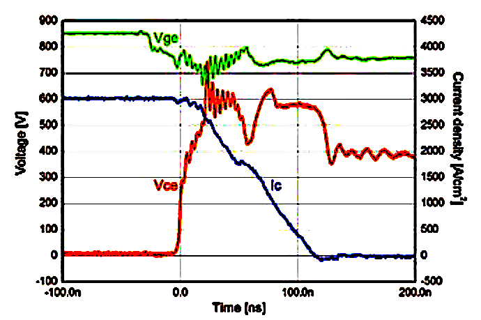
Figure 5: Dynamic lath up characteristics
About the Authors
Kyuhyun Lee worked as a director at Fairchild Semiconductor, a company pioneer in the manufacturing of transistors and of integrated circuits.
Sungmin Yang worked at Fairchild Semiconductor, a company pioneer in the manufacturing of transistors and of integrated circuits.
Sekyeong Lee worked as a principal design engineer at Fairchild Semiconductor, a company pioneer in the manufacturing of transistors and of integrated circuits.
Jiyong Lim worked as a staff design engineer at Fairchild Semiconductor then become principal engineer when company acquired by ON Semiconductor, a semiconductors supplier company.
Youngchul Choi worked as a director of technology development at Fairchild Semiconductor, a company pioneer in the manufacturing of transistors and of integrated circuits.
References
- A. Nakagawa, “Theoretical Investigation of Silicon Limit Characteristics of IGBT”, Proc. ISPSD’06, pp5-8, 2006
- Z. Chen, “Next Generation 600V CSTBTTM with an Advanced Fine Pattern and a Thin Wafer Process technologies”, Proc. ISPSD’12, pp25-28, 2012
- K. Matsushita “Low Gate Capacitance IEGT with Trench Shield Emitter (IEGT-TSE) Realizing High Frequency Operation”, Proc ISPSD’13, pp. 269-272, 2013
- M. Sumitomo, J. Asai, H. Sakane, K. Arakawa, Y. Higuchi, and M. Matsui, “Low loss IGBT with Partially Narrow Mesa Structure (PNM-IGBT)”, Proc. ISPSD’12, pp17-20, 2012 [5] K. Lee, “Optimized buffer layer for the high performance and enhanced short circuit immunity of Trench IGBT”, Proc. PCIM’13, pp351-356, 2013
This article originally appeared in the Bodo’s Power Systems magazine.