Facebook
 Google
 GitHub
 Linkedin
Dynamic Output Voltage Adjustment
This article describes different implementations of how to add the feature of adjusting the output voltage to nearly any switch-mode power supplies.
In some applications, a variable or adjustable supply voltage is a requirement. This can be for example the supply of a DC motor when PWM modulation is not possible due to EMI reasons. Another example is power supplies for audio amplifiers. Especially Class A and A/B amplifiers with only little load have large losses. By decreasing the supply voltage these losses can be reduced significantly.
Also for amplifiers working in Class D, a reduction of the supply voltage at low power increases the efficiency. This article describes different implementations of how to add the feature of adjusting the output voltage to nearly any switch mode power supplies (SMPS).
Error Amplifier
Each switch mode power supply has an integrated error amplifier. This can be a normal operational amplifier as shown in Figure 1 or a transconductance amplifier. The function is always identical and the implementation of the output voltage adjustment can be done in the same way, too. The error amplifier compares the voltage of the feedback voltage divider (VFB) with its internal reference (VREF) and sets the duty cycle (PWM) such that the difference is zero. As the reference voltage is typically in the range of a few hundred millivolts up to a single volt, the output voltage is divided by the feedback voltage divider (R1, R2). Between the input (FB) and the output (COMP) of the error amplifier, the compensation network is connected. Properly designed, it ensures good regulation of the output voltage under all line and load conditions.
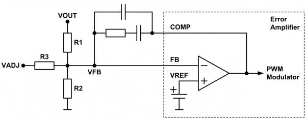
Figure 1: Error Amplifier
These external components are typically fixed, as the converter is designed for a non-variable output voltage. By applying an external voltage (VADJ) to the feedback of the error amplifier with a defined resistor (R3), an additional current is injected which flows via the low-side resistor (R2) to GND causing an additional voltage drop. This means, the voltage on the op amp’s input (FB) rises and the error amplifier reduces the duty cycle to get it back to the value of its reference voltage. This approach is called “analog” as an analog voltage is used to adjust the output voltage. Well implemented, the output voltage of the power supply is proportional to the analog adjustment voltage.
A short example shows the calculation of the three resistors.
- Minimum output voltage: VOUTmin = 5.0V
- Maximum output voltage: VOUTmax = 12.0V
- Minimum adjustment voltage: VADJmin = 0.0V
- Maximum adjustment voltage: VADJmax = 3.3V
- Reference voltage: VREF = 0.6V
When VADJ is set to 0.0V, resistor R3 is practically in parallel to R2. This means the output voltage has its maximum value. When VADJ is set to 5.0V, resistor R3 generates an additional current, which superimposes to the current of R1. In this case, the output voltage reaches its minimum value. Important to keep in mind that the minimum output voltage is limited by the reference voltage and cannot be lower than this value.
The three resistors can be easily determined in four steps:
First, the minimum current (IR1,min) through the high-side resistor R1 needs to be selected. Very low currents are susceptible to noise and very high currents cause needless losses. A typical value is 100µA, which is used in this example as well.
Now, the high-side resistor of the voltage divider is calculated.
`R_1=(VOUT_("min")-VREF)/I_(R1,min)`
`R_1=(5.0 V-0.6 V)/(100 μA)=44.0 kΩ`
The closest value of 44.2 kΩ is selected.
The next step is the calculation of resistor R3, which connects the external voltage with the feedback of the error amplifier.
`R_3=(R_1∙"VADJ"_("max"))/(VOUT_("max")-VREF-R_1∙I_(R1,min) )`
`R_3=(44.2 kΩ∙3.3 V)/(12.0 V-0.6 V-44.2 kΩ∙100 µA)=20.9 kΩ`
The closest value of 21.0 kΩ is selected
As R1 and R3 are known, the missing resistor R2 can be determined.
`R_2=(R_1∙R_3∙VREF)/(R_3∙VOUT_("max")-R_3∙VREF-R1∙VREF)`
`R_2=(44.2 kΩ∙21.0 kΩ∙0.6 V)/(21.0 kΩ∙12.0 V-21.0 kΩ∙0.6 V-44.2 kΩ∙0.6 V)=2.62 kΩ`
The closest value of 2.61 kΩ is selected.
The external voltage for adjusting the output voltage of the power supply can be generated in several ways. Most commonly a smoothened PWM signal or the output of a digital-to-analog converter (DAC) is used as shown in Figure 2.

Figure 2: Analog voltage generation
The first method is often used because it’s very simple and inexpensive. If an adjustable output voltage is needed, usually a microcontroller is somewhere in the system anyway. An output with pulse-width-modulation (PWM) capability generates a rectangular waveform, which is filtered by a low pass filter to convert it into the average DC voltage. To achieve a smooth analog voltage, the bandwidth of the low pass filter should be one decade or less below the frequency of the PWM signal. The step width of the adjustable output voltage depends directly on the resolution of the PWM signal.
Another method is the usage of a DAC like the DAC5311. If different adjustable power rails are needed and the amount of PWM outputs on a microcontroller is limited, several digital-to-analog converters can be controlled in parallel by the SPI bus. Here the step width also depends on the resolution of the DAC. This family of digital-to-analog converters offers a resolution from 8 bit (DAC5311) up to 16 bit (DAC8411), so it can cover any demand regarding the resolution of an adjustable output voltage for a switch mode power supply.
Digital Approach
For the “digital” approach, digital signals like the outputs of a microcontroller are used to directly change the output voltage of a power supply without the detour by a DAC for example. The idea behind this is pretty simple. By changing the resistance either of the high-side (R1) or the low-side resistor (R2), the output voltage can be manipulated.
It is important to notice, that the high-side resistor has an impact on the compensation, more precisely on the gain. If the value of this resistor is changed, the gain of the compensation network changes which can lead to instability and different behavior depending on the output voltage. Besides that, it is also not easy to change its resistance as it is floating and not referred to ground.
The better method is manipulating the low-side resistor. It has no impact on the compensation and thus the behavior of the converter will always stay the same. Additional resistors, which can be switched by logic-level FETs are put in parallel to the fixed low-side resistor (R2).
The example in Figure 3 shows a so-called VID interface (Dynamic Voltage Identification) with two bits. If a FET is driven by the digital output of a microcontroller, the corresponding resistor is switched in parallel to the fixed resistor R2. The overall resistance decreases and therefore the output voltage increases. With two bits, four different voltage levels can be set. Dependent on the demands, more steps can be added.

Figure 3: VID Interface
For this example the specification of the analog approach is used again:
First, the minimum current (IR1,min) through the high-side resistor R1 needs to be selected. 100µA is also used here.
Now, the high-side resistor of the voltage divider is calculated.
`R_1=(VOUT_("min")-VREF)/I_("R1,min")`
`R_1=(5.0 V-0.6 V)/(100 μA)=44.0 kΩ`
The closest value of 44.2 kΩ is selected.
R2 is the fixed low-side resistor, which is always connected between the feedback of the error amplifier and ground.
`R_2=(R_1∙VREF)/(VOUT_("min")-VREF)`
`R_2=(44.2 kΩ∙0.6 V)/(5.0 V-0.6 V)=6.03 kΩ`
The closest value of 6.04 kΩ is selected.
The number of steps depends on the number of bits of the VID interface. For example, four bits (0, 1, 2, 3) enable 16 steps. A single step is calculated with the following equation.
`VSTEP=(VOUT_("max")-VOUT_("min"))/(2^("BITS")-1)`
`VSTEP=(12.0 V-5.0 V)/( 2^4-1)=467 mV`
Theoretically, this calculation has to be done for each bit, so four times in this example (BIT 0, 1, 2, 3). But it is sufficient to do it only for bit 0 and then just use 1/2, 1/4 and 1/8 for the other three remaining values.
`R_(2,BITx)=1/((VOUT_("min")+2^("BIT")∙VSTEP-VREF)/(R_1∙VREF)-1/R_2 )`
`R_(2,BIT0)=1/((5.0V+2^0∙467 mV-0.6 V)/(44.2 kΩ∙0.6 V)-1/(6.04 kΩ))=55.7 kΩ`
The closest value of 56.2 kΩ is selected.
With the four switchable resistors parallel to the fixed resistor R2, the output voltage can be set between 5.0V and 12.0V in 16 steps.
A similar, but a more integrated solution can be implemented with a digital potentiometer like the TPL0401A-10 shown in Figure 4.
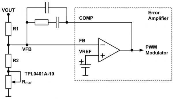
Figure 4: Digital Potentiometer
The potentiometer RPOT is in series with the low side resistor R2 and controlled by either I2C or SPI. This specific device has 128 taps, so its functionality is similar to a discrete VID interface with 7 bits. It is important not to use it as the feedback voltage divider itself, otherwise, the high-side resistance will change depending on the output voltage and thus have an impact on the compensation as explained at the beginning.
Digital-Analog Approach
The third approach is the “digital-analog”, which uses a combination of both solutions shown. It is based on Texas Instruments LM10011V VID programmable current DAC. This device has four logic inputs, which are driven in the same manner as described in the digital approach. The output of the device is not a voltage, but a current, which is fed directly into the low-side resistor R2 of the voltage divider as shown in Figure 5. Similar to the analog approach, this programmable current in the range of 0 to 59.2 µA causes an additional voltage drop on the low-side resistor and thus controls the output voltage of the power supply.
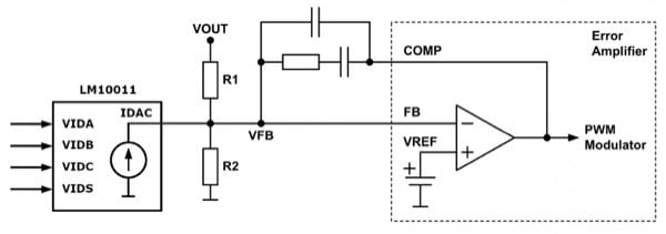
Figure 5: LM10011 VID Programmable Current DAC
It can be used either in 4 bit or 6-bit mode, thus providing 16 and respectively 64 steps for adjustment of the output voltage. The advantage is the smaller solution size compared to a discrete setup and its compatibility to TI’s TMS320 DSPs which control their supply voltage autonomously dependent on the load.
Conclusion
Typically, a power supply provides only a fixed output voltage. But in some applications, it is necessary or desirable to change this voltage in a certain range. This article describes three different approaches to expanding this functionality to practically all power supplies. Almost any signals like PWM, simple logic, SPI/I2C or dedicated VID interfaces can be used. The speed of change of the output voltage depends mainly on the bandwidth of the converter and less of the control circuit.
About the Author
Matthias Ulmann was born in Ulm, Germany, in 1980. He was awarded a degree in electrical engineering from the University of Ulm in 2006. After working for several years in the field of motor control and solar inverters (specialized in IGBT-drivers), he joined TIs’ Analog Academy for a one-year trainee program. Since 2010 he has worked in the EMEA Design Services Group as a Reference Design Engineer in Freising, Germany. His design activity includes isolated and non-isolated DC/DC converters for all application segments. He was elected “Member, Group Technical Staff” in 2015.
This article originally appeared in the Bodo’s Power Systems magazine.