Facebook
 Google
 GitHub
 Linkedin
Automotive High Capacity Power Module
The automotive industry is currently undergoing a tremendous change. Due to higher awareness of the negative impact of air pollutants on human health and
The automotive industry is currently undergoing a tremendous change. Due to higher awareness of the negative impact of air pollutants on human health and the climate change due to CO2 emission, electrification in passenger cars, busses as well as commercial vehicles is becoming ever more important. Mitsubishi Electric as one of the pioneers in electrified vehicles, which started mass production of automotive power modules in 1997, is today delivering optimal power module solutions for all power classes.
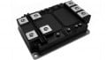
With the J1-Series power modules, Mitsubishi Electric is delivering a family of automotive-grade standard modules to meet different power classes. For the high power variant, our customers can choose between the CT1000CJ1B060 with 650 V chips or the CT600CJ1B120 with 1200 V chips. With current ratings of 1000 A for the CT1000CJ1B060 and 600 A for the CT600CJ1B120, Mitsubishi Electric offers a solution for the highest power demands.
Our long experience in the market of electromobility was incorporated in the development of the J1 power module family to meet the requirements of the automotive industry for high efficiency and reliability, high power density and low weight. In this article it will be explained how these requirements are met.
| Type Name | CT1000CJ1B060 | CT600CJ1B120 |
| Ratings (IC / VCES) | 1000 A / 650 V | 600 A / 1200 V |
| Circuit /Sensing Function | 6 in 1Temperature sensor (all phases)Current sensor (all phases) | 6 in 1Temperature sensor (all phases)Current sensor (all phases) |
| Package Size | 163 x 124.5 x 20.9 (mm) | 163 x 124.5 x 20.9 (mm) |
Table 1: High power J1-Series Line-up

Figure 1: J1 series power module in high power package

Figure 2: Circuit diagram of J1 module high power package
Mitsubishi 7th Generation IGBT chip
The 7th generation of Mitsubishi Electric’s IGBT chips features the Carrier Stored Trench-Gate Bipolar Transistor (CSTBTTM) technology, reducing the power losses significantly as compared to previous IGBT generations. Important factors are the low collector-emitter saturation voltage VCE(sat) and the reduced turn-OFF switching losses of the latest chip generation. This is achieved by the ultra-thin chip technology. It is supported by incorporation of on-chip sensors for real-time protection functions such as short-circuit detection, which reacts significantly faster than the conventional desaturation detection. Additionally, a temperature sensor is integrated at the chip center for over-temperature detection and optimal utilization of the chip performance.
The good performance of the IGBT chip is supported by an optimized Relaxed Field of Cathode (RFC) diode in parallel, which has low forward voltage drop and soft reverse recovery. Because of the better reverse recovery behavior of the RFC diode, the IGBT can be turned on faster which also reduces the turn-ON losses.Below pictures show a schematic of the IGBT chip with the location of the temperature sensors, which are included in each chip of the J1-series modules and a waveform of the real-time short circuit detection.

Figure 3: Improvement of Conduction and Turn-OFF losses by 7th generation IGBT
Direct Lead Bonding (DLB) Package Technology
Conventional power modules use bond wires to contact the top sides of the chips. Instead, Mitsubishi Electric J1-Series power modules feature the Direct-Lead-Bonding (DLB) technology which replaces the bond wires by copper lead frames to conduct the high currents. While conventional bond wires are prone to lift-off under power cycling, this failure mechanism cannot be seen in the DLB technology, leading to a significantly higher power cycling lifetime. This is an important factor for the lifetime of automotive inverters because the dynamic driving profiles and harsh environmental conditions lead to frequent high temperature swings.
Besides that, the DLB technology provides several other advantages: The high contact area between the chip and the lead frame reduces the temperature gradient between the chip hotspot and the chip edges and generally leads to a better conduction of heat away from the chip.

Figure 4: Location of sensors and signal terminals on IGBT chip

Figure 5: Waveform example of arm-short of CT1000CJ1B060
Internal Package Layout
Although the J1-Series automotive modules are designed to be comparably compact, with increasing power rating the package size increases which typically leads to an increase in the parasitic package inductance. The resulting switching voltage spikes limit the maximum switching speed of the IGBTs and hence increase the switching losses. Nevertheless, the package of the high power J1-Series was optimized to reduce the package inductance by a laminated bus bar layout with parallel current paths to cancel the magnetic flux. The low parasitic inductance is again supported by the DLB technology using large area copper frames.Another outstanding feature of the J1-Series package design is the elimination of the solder layer between the substrate and the baseplate. This results in a reduction of the thermal resistance and an improvement of the thermal cycling capability.
Direct Cooled Pin-Fin Aluminum Baseplate
In automotive applications liquid cooling of the drivetrain components such as the traction inverter or electrical machine is standard. For a compact design with good thermal characteristics the J1-Series modules are equipped with an aluminum baseplate with Pin-Fin structure for direct liquid cooling. Using aluminum as a baseplate and Pin-Fin material reduces the weight of the module and additionally has higher durability when exposed to liquid coolants than for example copper, which needs additional plating. Chip Parallel ConnectionIn order to reach the high output current of the power module, chips are operated in parallel. The module is designed with respect to optimizing the current balance between parallel chips. One factor is that the internal structure was optimized, so that the DLB is the emitter side connection of the chips and that it minimizes the difference of the inductances between the parallel chips. Figure 9 shows a comparison between using a single chip and two chips in parallel. Looking at the output of the current sensor on one of the chips, it can be seen that for the same measured value the output current is nearly doubled if two chips are operated in parallel. This proves the good current sharing of the parallel connection.

Figure 6: Comparison of conventional wire bond and Direct-lead-bonding technology

Figure 7: Cross section of J1-Series high power package

Figure 8: Parasitic inductance comparison of High Power J1-Series and conventional design

Figure 9: Current distribution characteristics between two chips of CT1000CJ1B060
Inverter Simulation Results
Performance of the J1 high power Module was evaluated by inverter simulation. Below graphs show the simulated junction temperature of the IGBT chips for different inverter output currents at a switching frequency of fc = 5 kHz, a coolant temperature of Tw = 65 °C and a flow rate of 10 L/min. The DC-link voltages were set to VDC = 300 V (for CT1000CJ1B060) and VDC = 600 V (for CT600CJ1B120) respectively.

Figure 10: Inverter Mode Simulation results for CT1000CJ1B060 J1-module

Figure 11: Inverter Mode Simulation results for CT600CJ1B120-module
The simulation shows the high current capability of both variants. The CT1000CJ1B060 can reach an output current of IO = 700 ARMS with staying significantly below the maximum continuous junction temperature, while the CT600CJ1B120 reaches more than IO = 400 ARMS.
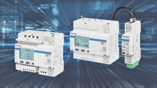
Evaluation Kit
A complete evaluation kit can be provided together with the module for laboratory testing. It includes a cooling jacket to utilize the direct water cooling of the power module, a DC link capacitor and a driver board with a driver IC (M81605JFP) optimized to utilize the full functionality of the J1-Series by evaluating the on-chip sensors.
Summary
With the J1-Series Mitsubishi Electric provides a range of automotive grade power modules for medium to high power drivetrain applications. This article was focusing on the high power variant which is available in the voltage classes 650 V and 1200 V and was designed to meet the requirements of the automotive industry. The module achieves outstanding power density, efficiency and due to the Direct-Lead-Bonding technology also high lifetime.
About the Authors
Rene Spenke is an applications engineer in automotive power semiconductors with bei Mitsubishi Electric Europe. Spenke has published articles on subjects such as "Automotive High Capacity Power Modules" and "Bidirectional dual active bridge converter using a tap changer for extended voltage ranges."
Khalid H. Hussein is a Manager at Mitsubishi Electric Europe B.V. He has 23 years experience in the power electronics engineering and renewable energy utilization fields. Hussein also holds a PhD in Electrical & Electronics Engineering alongside an MBA in Sustainable Management.
References
- “A New High Capacity Compact Power Modules for high power EV/HEV inverters”, Seiichiro Inokuchi, Shoji Saito, Arata Izuka, Yuki Hata, Shinji Hatae
- “Mitsubishi Electric to Expand Lineup of J1-Series High-power Semiconductor Modules”, Mitsubishi Electric Corporation press release No. 2930, Tokyo, May 12 2015
- “Large Capacity Power Module Packaging Technology for Automotive Inverter Applications”, PCIM Europe 2018, Yuki Haka, Shoji Saito, Seiichiro Inokuchi, Shinji Hatae
- “High Performance 7th Generation chip installed Power Module for EV/HEV Inverters”, PCIM 2015, Yosuke Nakata, Mikio Ishihara, Noboru Miyamoto, Khalid Hussein, Thomas Radke, Marco Honsberg, Shinsuke Godo
This article originally appeared in the Bodo’s Power Systems magazine.
Related Content