Facebook
 Google
 GitHub
 Linkedin
High-Power Next Core for Solar, Wind and Rail
The High Power next Core module is the latest in Fuji's high-power portfolio, covering a range of industrial applications, predominantly for solar, wind, and rail.
This article is published by EE Power as part of an exclusive digital content partnership with Bodo’s Power Systems.
In 1923, a company now called Fuji Electric Co., Ltd. was founded as a joint venture of Japanese Furukawa Electric Co., Ltd. and German Siemens AG. Throughout the 100 years of company history, many branches and markets have been penetrated with electric equipment. Within the last decades, sustainability and a stable supply of clean energy came into focus. The HPnC (High Power next Core) module from Fuji Electric is the latest in the high-power portfolio. It covers a range of industrial applications, predominantly for solar, wind, and rail. Different chip technologies, Silicon and Silicon Carbide, with trench gate structures, are applied to fulfill the demand for energy efficiency and performance.

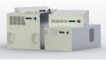
Figure 1. HPnC package with dimensions. Image used courtesy of Bodo’s Power Systems [PDF]
HPnC for Traction Market
The traction market also strives for power semiconductors with increased efficiency and lower weight, especially with the blocking voltage of 3300 V. By using SiC instead of Si technology, almost doubling the power density can be achieved. This performance boost combined with the option of an omitted SiC-SBD (SchottkyBarrier-Diode) for further MOSFET space – 15% gain has been achieved – is paving the way for SiC-dominated propulsion converters in traction application.
The HPnC’s low internal package inductance with only 10 nH is also suitable for high-speed switching at the lowest switching losses and only minor oscillations. The rolling stock also has harsher requirements than industrial applications: The package complies with parameters like isolation capability, partial discharge, fire, and smoke as defined in common standards (EN 50124-1, EN 45545- 2). Especially the dTc power cycling capability needs to be high for the long acceleration and deceleration phases. For this purpose, another baseplate material, MgSiC, is chosen over the standard copper type used in the industrial version of the HPnC, offering better thermal performance due to lower thermal resistance. MgSiC is superior in terms of thermal resistance compared to AlSiC baseplates used by competing products while maintaining the same mechanical robustness.
A comparison of chip configurations in SiC-HPnC modules with 750 A/3300 V is summarized in Table 1. The finer trench gate structure of the 2nd gen technology results in a lower on-state voltage VDS(on) value compared to the 1st-gen SiC-MOSFETs. The SiC-SBD is optional since the MOSFET body diode can handle the currents. However, keeping the body diode in the module brings some benefits, which are increasing the I²t capability and lowering the VSD. As various operating conditions are present, the module chipset is versatile and comes with or without the SiC-SBD. The recommended gate voltages for 2nd gen technology are the same as Si-based modules to simplify the switch from Si to SiC technology.
A comparison of the dynamic characteristics of 1st and 2nd Gen SiC technology versus the latest Si technology is shown in Figure 2, where the gate resistances have been chosen to get the same di/dt for turnoff, turn-on, and reverse recovery. Additionally, the current displayed on the second vertical axis is normalized. The SiC tail currents are negligible for the turnoff waveforms, and the voltage rise is much faster than the Si module. In the case of turn-on and reverse recovery, the peak currents are less distinctive for the SiC modules. The switching energies Eoff, Eon and Err are 81%, 66%, and 98% lower in the SiC modules than in the Si modules. There is no significant difference between the switching energies of 1st-gen and 2nd-gen SiC modules with SBDs.
Table 1. Comparison of different chip configurations (1st and 2nd gen) in SiC-HPnC modules with 750 A/3300 V.
| 1st Gen trench gate SiC MOSFET | 2nd Gen trench gate SiC MOSFET | 2nd Gen trench gate SiC MOSFET | |
| With SBD | With SBD | Without SBD | |
| VDS(on) at 150 °C | 3.80 V (Vgs=20V, Id=750A) | 3.40 V (Vgs=15V, Id=750A) | 3.40 V (Vgs=15V, Id=750A) |
| VSD at 150 °C | 2.45 V (Vgs=20V, Id=750A) | 2.25 V (Vgs=15V, Id=750A) | 3.40 V (Vgs=15V, Id=750A) |
| VSD at 150 °C | 3.30 V (Vgs=-3V, Id=750A) | 3.30 V (Vgs=-3V, Id=750A) | 4.80 V (Vgs=15V, Id=750A) |
| Vgs(th) at 25 °C | 4.7 V | 5.0 V | 5.0 V |
| I²t (VGS=-3V,Tvj=25°C) | 70.2 kA²s | 70.2 kA²s | 42.9 kA²s |
| Gate voltage level | +20/-3 V | +15/-3 V | +15/-3 V |

(a)

(b)

(c)
Figure 2. Turn off (a), turn on (b) and reverse recovery (c) waveforms of different SiC and Si modules. Images used courtesy of Bodo’s Power Systems [PDF]
There is, however, a discrepancy between 2nd Gen SiC modules with and without SBDs. Figure 3 depicts the switching waveforms of turnoff, turn-on and reverse recovery for a rated current of 750 A. Clearly visible is that the turnoff and turn-on waveforms are almost identical. In contrast, the recovery waveform is different and a much steeper rise of the Source-Drain voltage can be noted for the module without SBD. These facts are supported by the related switching energies and dv/dt values obtained from the graphs: the turn-on losses are 319.2 mJ for the module with SBD and 326.0 mJ for the module without SBD; for turnoff, the values are 218.4 and 226.9 mJ, and in case of reverse recovery 9.8 and 8.5 mJ can be reported. In the case of reverse recovery, a slightly lower switching loss is observed for the module with SBD contrary to higher values for turn-on and turn-off. The biggest difference is the reverse recovery dv/dt: 26.2 to 39.7 kV/µs for the modules with and without SBD.

(a)

(b)

(c)
Figure 3. Turn off (a), turn on (b) and reverse recovery (c) waveforms of different 1st and 2nd-gen SiC modules. Images used courtesy of Bodo’s Power Systems [PDF]
Using the Fuji IGBT simulator, some simulated losses from a real traction mission profile can be compared for various modules. The operating conditions are taken from a 180 kW and 1500 VDC train, which uses the following parameters: Vcc = 1500 V, Io = 510 Arms, cosφ = +/-0.85, λ = 1.0, fc = 1 kHz, Tvj = 150 °C for acceleration and deceleration. For this example, the following modules were chosen: 450 A/3300 V Si module (two in parallel connection), 750 A/3300 V 1st Gen SiC module with SBDs, 750 A/ 3300 V 2nd Gen SiC modules with and without SBDs, and 850 A/3300 V 2nd gen SiC module without SBDs.
Table. Figure 4. Preliminary HPnC product lineup for modules being under consideration and development.
| Voltage | Application | Chip | Current | |||||||
| 450 A | 600 A | 750 A | 850 A | 1000 A | 1200 A | 1500 A | 1800 A | |||
| 1700 V | Industrial | Si | √ | √ | √ | |||||
| SiC w/ SBD | √ | √ | √ | |||||||
| Traction | Si | √ | √ | |||||||
| SiC w/ SBD | √ | √ | √ | |||||||
| 3300 V | Traction | Si | √ | |||||||
| SiC w/ & w/o SBD | √ | √ | ||||||||
As a result of the acceleration case, the total loss dissipation of 1st gen SiC module is 7% bigger than the alternative of two parallel Si-IGBT modules. The 2nd gen SiC modules with SBDs are 5% lower compared to Si modules with two parallel modules. The lowest losses of 644.1 W were achieved by the 2nd gen SiC module without SBDs and a rating of 850 A/3300 V. The total power dissipation of the 2nd gen SiC module with a nominal rating of 850 A without SBDs is 8% lower than the 2nd gen SiC module with SBDs with a nominal rating of 750 A.
The picture for the deceleration case is different, where the 2nd gen SiC module with SBDs and 750 A creates the lowest losses of 601.4 W due to the SBD characteristic. This finding results in the statement that SiC modules with SBDs and without SBDs are available to satisfy the various operating conditions.
Lineup Plan
The package itself is suitable for traction use. Current considerations of an industrial version rely on the market’s feedback and might be realized at a later point in time. There are slight but important differences in conditioning the traction module for higher thermal reliability and the harsher environment. The major change affects the baseplate, MgSiC instead of Cu, and was already mentioned above. The maximum temperature is limited to Tvj,op(max) = 150 °C and Tc(max) = 125 °C, where in general, the industrial modules are each approved for 25 °C higher. The isolation voltage also differs: VAC,isol = 6 kV (1 min) for the traction module instead of 4 kV (1 min).
The preliminary lineup is split into the two application fields, industrial and traction, and Si and SiC technology, as shown in Figure 4.
2300 V Device for 1500 VDC Applications
Since chips with a nominal breakdown voltage of 1700 V cannot be used in 1500 VDC applications and 3300 V chips have too high on-state voltage and switching losses, a new class of 2300 V chips is introduced. Thus, the upcoming 2300 V devices will enable efficient and cost-effective two-level topologies over the three-level NPC topologies with 1200 V devices. As the latest generation of wind turbines are equipped with 900 VAC, compared to the predecessor 690 VAC systems, realizing 1500 VDC in the DC-link is key for a power upgrade. In addition, the solar installations and their grid balancing batteries will subsequently be shifted to 1500 VDC.
The 2300 V chips are the latest 7th generation “X-series” Si technology or 2nd/3rd generation SiC technology. Both technologies have high breakdown voltages, low losses, and high-temperature capability, whereas the SiC MOSFET is inherently superior in high switching frequency applications.
The 2300 V Si-IGBT has a trench-gate structure, and a Field-Stop layer is incorporated in the chip backside layer. The overall chip thickness could be reduced compared to the previous generation. For the 2300 V SiC MOSFET, additional improvements were accomplished, like a narrower cell pitch and increased channel mobility. The MOSFET’s body diode can handle the current which would normally pass through the additionally installed, anti-parallel connected, free-wheeling diode (SBD). The 2nd gen SiC-Trench-Gate-MOSFET cell pitch could be reduced by 35% compared to the predecessor 1st gen technology. The schematics can be seen in Figure 5.

Figure 5. Schematic cross-section of Si-IGBT (left) and SiC-MOSFET (right) chip technology. Image used courtesy of Bodo’s Power Systems [PDF]
The static characteristics of the 2300 V chips at Tvj = 150 °C are: VCE(on) = 2.55 V (Si-IGBT) and VF = 2.15 V (Si-FWD), and VDS(on) = VSD(on) = 2.40 V (SiC MOSFET). The recommended gate voltages are +15/-15 V for the Si IGBT and +15/-3 V for the SiC MOSFET.
Figure 6 depicts the forward voltages VCE,sat and VDS(on) versus the currents IC and ID. The red dashed line indicates the nominal current rating. The 2300 V chips in 2-level topology with Si IGBT and SiC MOSFET have a 33 % and 37 % lower on-state voltage than the 3-level NPC topology with 1200 V Si-IGBT chips. The difference can be increased by operating at lower current ratings.

Figure 6. Simulated I-V curves for Si and SiC devices of different voltage classes at 150 °C. Image used courtesy of Bodo’s Power Systems [PDF]
In Figure 7, the free-wheeling behavior of the chips is shown. The Si-FWD and the SiC MOSFET forward voltage VF and VSD(on) are plotted as a function of IF and ISD in the same way as in Figure 6. Here, the advantage over the three-level NPC topology with 1200 V SiIGBT is 33% and 26% for the 2300 V Si IGBT and SiC MOSFET.

Figure 7. Simulated I-V curves for Si-FWD and SiC-MOSFET chips of different voltage classes at 150 °C. Image used courtesy of Bodo’s Power Systems [PDF]
By comparing two-level and three-level NPC topology, it becomes clear which advantages the 2300 V chips have instead of using several 1200 V chips. In theory, three modules must be connected and controlled by an individual gate driver channel each in a three-level inverter, for 12 gate driver channels. In the case of A-NPC topology, two additional IGBT switches are required for 18 gate driver channels. As opposed to this, a two-level topology requires only one module taking one-third of the footprint and 6 gate driver channels. This leads to less space needed and lesser costs. Another advantage the two-level topology has is the lower commutation inductance since the commutation current passes through a single module. The ultimate improvement is eventually using SiC technology, with which the total losses can be decreased by more than half.
This article originally appeared in Bodo’s Power Systems [PDF] magazine.