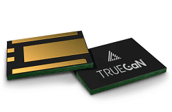
AIXTRON SE will provide high-end MOCVD technology to NexGen Power Systems Inc. for the continued development of GaN-based electronic devices enabling more compact, lighter and cost-efficient power conversion systems. For this purpose NexGen has ordered AIXTRON's AIX G5 HT planetary platform, scheduled for shipment in Q3/2018.
Considering yield and cost of ownership, the AIX G5 HT platform is the tool of record for all advanced GaN applications. As the only MOCVD system in the market embedding wafer level control, the AIX G5 is the most efficient tool for the epitaxy of GaN-on-GaN, GaN-on-Si and GaN-on-SiC used for power electronic and RF applications.
The fully-automated tool offers in-situ cleaning for best process robustness and defect control while it is also equipped with the latest Laytec InSide P400 UV Pyrometer for non-contact temperature measurement. Coupled with AIXTRON's Auto Feed-Forward (AFF) individual on-wafer temperature control, this enables a matching of all epitaxial wafers - within a run as well as run-to-run.
Dinesh Ramanathan, CEO of NexGen Power Systems, says: "Our disruptive True GaN™ VJFET (Vertical Junction Field Effect Transistor) technology is able to outperform silicon, silicon carbide or GaN-on-Silicon technology by providing higher breakdown voltage, lower on-resistance and higher switching frequency.
"NexGen's True GaN™ power devices enable the design of compact power conversion systems while increasing their efficiency with applications in data center power supplies, motor drivers, solar inverters and electric car drive-trains.
"AIXTRON's planetary technology in combination with its batch reactor concept will provide us both the performance control we need as well as the cost effectiveness to ensure a rapid adoption of our groundbreaking power devices," concluded Ramanathan.
"We are looking forward to support NexGen's efforts to revolutionize existing power conversion systems. In recent years, our AIX G5 HT planetary tools have built a solid reputation as precise, reliable and cost-efficient manufacturing equipment in the semiconductor industry - unlocking a more rapid adoption of GaN devices against their silicon equivalents", comments Dr. Felix Grawert, President of AIXTRON SE.
The figure below shows the schematics of True GaN™ vertical junction field-effect transistor (VJFET) and GaN-on-Si high electron mobility transistor (HEMT). In case of True GaN, the substrate and the epitaxial layers are both GaN with extremely low defect densities. For higher breakdown voltage scaling in True GaN™ VJFET, drift thickness is scaled up with no 2-D area penalty.
 Schematic of True GaN VJFET and GaN-on-Si HEMT. Dotted green lines denote the electron conduction path. (click on figure to enlarge)
NexGen Power Systems has successfully demonstrated drift thickness of >40µm producing diodes with breakdown voltage >4000V and specific on-resistance 2.8mΩ.cm2. For same RDSON, GaN die size is 4X smaller than GaN-on-Si HEMT at for BV=600V and 7X smaller for BV=1200V. True GaN™ VJFET has avalanche capability that allows reverse biased voltage to exceed the maximum BV value for a specified energy and current limitations.
True GaN VJFET also does not suffer from current collapse phenomenon because it does not rely on 2DEG (sheet of electron charge due to polarization at the interface between AlGaN and GaN).
Some salient features of True GaN technology:
- Homoepitaxial growth on GaN substrate
- Patented the most optimal spectrum of these offcut angles that results in best morphology and thus best device performance.
- Flexibility to use bulk GaN substrates from all major vendors
- Ability to produce ultra-low doped n-GaN
- Proprietary methods to control Mg doping during growth to grade p-n junctions or to produce sharp p-n junction profiles as desired
- Proprietary highly planarizing regrowth process with very low surface roughness


