Facebook
 Google
 GitHub
 Linkedin
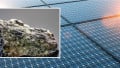
Low-cost Wafers for Solar Cells
Silicon wafers are the heart of solar cells. However, manufacturing them is not cheap. Over 50 percent of the pure silicon used is machined into dust. A new manufacturing technique developed by Fraunhofer researchers puts an end to these material losses, with raw material savings of 50 percent along with an 80 percent reduction in energy costs. A key component of these is thin silicon wafers. The manufacture of these wafers is very time and energy consuming, and correspondingly expensive. What's more, around half of the silicon is lost during production of the wafers. The current price for polysilicon is around 15 euros per kilogram, which means that for every kilogram of polysilicon used, about 8 euros' worth of the material ends up as contaminated and therefore unusable silicon.
This is not the case with the new process developed by researchers at the Fraunhofer Institute for Solar Energy Systems ISE in Freiburg. “With our method, we can avoid almost all of the losses that occur during the conventional production process,†says researcher Dr. Stefan Janz at the ISE. “This means we are reducing material losses by 50 percent while using 80 percent less energy.â€
Recently NexWafe GmbH was spun out of the Fraunhofer Institute for Solar Energy Systems ISE, in order to bring the Institute’s kerfless EpiWafer technology to the market and rapid commercialization. In the EpiWafer technology, a thick crystalline silicon layer is epitaxially deposited and subsequently detached after growth to produce a freestanding wafer of standard thickness. Due to the radical changes in the manufacturing value chain, EpiWafers can be produced at an appreciably lower cost compared to the traditional wafer manufacturing process. The EpiWafer is a direct substitute for conventional n- or p-doped silicon mono-crystalline wafers.
Now, Fraunhofer ISE reports on substantial progress in the development of its EpiWafers, which are seen as a drop-in replacement for conventional Cz wafers. Fraunhofer ISE’s research team in co-operation with NexWafe has optimized all production steps for the EpiWafer. Analysis of the new n-doped EpiWafers shows that mean minority carrier lifetimes are above 1000μs, indicating the same quality as n-type Cz wafers. Solar cells processed on these EpiWafers yield 20% efficiency, independently confirmed at the Fraunhofer ISE CalLab.
“I am elated about this fantastic result,†says Dr. Stefan Janz, Head of the Department of Silicon Materials. “This success attests to our fast progress made in only a few months since focusing on EpiWafers.†The solar cells achieve a short-circuit current of 39.6 mA/cm2, a world-record value for epitaxially grown silicon solar cells. The new results will be presented during the coming European PVSEC in Hamburg.
Dr. Stefan Reber, CEO of NexWafe, is also very excited about the new results: “These values demonstrate that our EpiWafer technology is a game-changing technology. It accelerates the shift of the market towards high efficiency modules by providing high quality drop-in mono-crystalline EpiWafers at a very competitive price.â€
In order to understand how the researchers have accomplished this, it is worth taking a look at the conventional manufacturing process for silicon wafers. This process begins with an impure chunk of silicon. The impure silicon is liquefied and purified by adding chlorine. The material thus created is known as chlorosilane. If hydrogen is added to the resulting gas it is then transformed again into high-purity polysilicon. But this is not the crystalline form needed for solar cells. Therefore, the resulting silicon chunks are again broken up, melted at 1450 degrees Celsius, grown using different methods and transferred into silicon ingots weighing 200 to over 1000 kilograms. From these, square-shaped blocks are created and ultimately sawed into small wafers.
Similarly, in the new process researchers first manufacture chlorosilane, heat it to over 1000 degrees Celsius and mix it with hydrogen. “We don’t let the silicon just grow randomly, instead we immediately coax it into the desired crystalline form,†explains Janz. This is done through chemical vapor deposition. Here, the gaseous silicon flows past the substrate –itself a silicon wafer – and coats its surface. In this way, the wafer grows atomic layer by atomic layer. To make the new wafer easily separable from the substrate, researchers will introduce a mechanical breakpoint beforehand in the form of porous silicon. These substrates can be reused several dozen times.
Not only do the substrates serve as a “backing plateâ€, they also provide the necessary crystal information. This is because for solar cells, a silicon crystal is needed in which the atoms are arranged in a regular array, much as they are in a diamond. The substrate informs the atoms, so to speak, about how they should arrange themselves from the gaseous silicon. “In this way we get a very good monocrystal, which is the best type of crystal, and the wafers are of the same quality as those produced using conventional methods,†says Janz. In short, the wafer grows exactly how the researchers want it to, with no need for cumbersome sawing – a process step that wastes almost half of the high-purity input material.
Another advantage of the new process is that it allows the wafers to be made as thin as desired. With the conventional process, the silicon wafers must be at least 150 to 200 micrometers thick, as otherwise the cutting losses would be too high. But solar cells can make do with far thinner wafers. And the thinner the wafer, the cheaper the solar cell. So the new process saves material in two ways: by avoiding a wasteful wafer manufacturing process and by permitting reduced wafer thicknesses. These gains really add up because cutting the cost of the wafer in half brings down the cost of the entire solar module by 20 percent.
As of June 2015, NexWafe has assumed responsibility for bringing this new wafer production technique to market. “In the pilot phase of this technology we’re working in close cooperation with our colleagues at Fraunhofer ISE,†says Dr. Stefan Reber, NexWafe CEO. The completion of the factory and the start of mass production for the lower-cost wafers are slated for late 2017.