Facebook
 Google
 GitHub
 Linkedin
Graphene Flagship Develops Method for Graphene Integration into Silicon Wafers
The Graphene Flagship’s industry and academic partners combined their knowledge and expertise to integrate high-quality graphene into silicon wafers for the first time.
The Future and Emerging Technology Flagship is funded by the European Union. It brings together researchers from academia and industry to take innovations in graphene technologies from the lab and bring them to commercial applications.
The Graphene Flagship is supported by €1 billion in funding and its core consortium includes around 170 academic and industrial research groups in 22 countries.
Recently, the Flagship developed a wafer-scale fabrication technology that can integrate graphene into silicon wafers. This was made possible with predetermined graphene single-crystal templates. The processes used to develop the technology can be fully automated and the technology itself could pave the way toward large-scale production of graphene-enabled photonic devices.

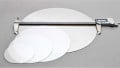
Partners from the Graphene Flagship develop a way to integrate graphene into silicon wafers. Image used courtesy of The Graphene Flagship
Graphene-Powered Telecommunications
\Research into technological innovations of the future tends to have a focus on reducing production costs during manufacturing, reducing the size and amount of materials needed for the fabrication of a particular device or product. Such factors have a direct effect on the level of greenhouse gases emitted, which in turn influences environmental impact. Today, certain telecommunications devices requiring 5G, need to meet the requirements of ultra-high-speed communications and high energy consumption. Although silicon and germanium have proven to show attractive qualities for developing such devices, the new kid on the block, graphene, may beat them to the post. “In graphene, almost all the energy of light can be converted into electric signals, which massively reduces power consumption and maximizes efficiency,” commented research co-lead Marco Romagnoli in a recent press release. Romagnoli is from Graphene Flagship partner CNIT, linked third party INPHOTEC, and associated member CamGraphiC.
Graphene Flagship Collaboration
The research, published in the journal ACS Nano, was a concerted effort between several Graphene Flagship partner institutions. Partners involved included the National Inter-University Consortium for Telecommunications (CNIT) and the Istituto Italiano di Tecnologia (IIT), in Italy, the Cambridge Graphene Centre at the University of Cambridge, UK, and Graphene Flagship spin-off CamGraphIC.

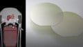
Image used courtesy of The Graphene Flagship
Romagnoli explained that the methods employed within the research enabled the team to “obtain over 12000 graphene crystals in one wafer, matching the exact configuration and disposition we need for graphene-enabled photonic devices.” The researchers used a technique called chemical vapor deposition (CVD) and transferred the graphene in a way that provided 80% of coverage of the device area.
In another study, Graphene Flagship partners used this approach to physically apply the graphene-based technology and designed high-speed graphene photodetectors.“Together, these advances will accelerate the commercial implementation of graphene-based photonic devices,” said research co-lead Camilla Coletti, coordinator of IIT’s Graphene Labs.
Advantages of Graphene-Based Photonic Devices
Graphene-enabled photonic devices can provide ultra-broadband communications with the ability to absorb light from ultraviolet to the far-infrared. Additionally, graphene devices can have ultra-high mobility of carriers including electrons and holes.This can greatly enhance data transmission and even break the record among the top-performing ethernet networks that operate at around 100 gigabits per second.
In the same press release, Graphene Flagship Leader for Photonics and Optoelectronics, Frank Koppens, said: “This is the first time that high-quality graphene has been integrated on the wafer-scale. The work shows direct relevance by revealing high-yield and high-speed absorption modulators. These impressive achievements bring commercialisation of graphene devices into 5G communications very close.”
Developing a wafer-scale process for integrating graphene into silicon wafers is key step in the direction toward more efficient, and more environmentally sustainable telecom and datacom communications.