Facebook
 Google
 GitHub
 Linkedin
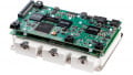
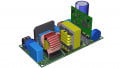
GaN-Based Interleaved CCM Totem Pole Bridgeless PFC Reference Design
The TIDM-1007 reference design from Texas Instruments illustrates a method to control an interleaved continuous conduction mode (CCM) totem pole (TTPL) bridgeless power factor correction power stage using a C2000™ MCU and the LMG3410, a single-channel GaN power stage containing a 70-mΩ, 600-V GaN power transistor and specialized driver.
Targeted applications include onboard chargers for electric vehicles, telecom rectifiers, motor drives, welding power supplies and other industrial ac-powered converters.
The design supports phase shedding and adaptive dead time for efficiency improvements, input cap compensation scheme for improved power factor at light loads, and non-linear voltage loop to reduce voltage spikes under transient.
The hardware and software available with this reference design accelerates time to market. Features of this reference design include:
- Interleaved, 3.3-kW, single-phase, bridgeless CCM totem pole PFC stage
- 100-kHz pwm switching
- Programmable output voltage, 380-Vdc nominal
- Less than 2% THD
- Greater than 98% peak efficiency
- powerSUITE™ support for easy adaptation of design for user requirement
- Software frequency response analyzer (SFRA) for quick measurement of open-loop gain
- Soft starting of pwm for reduced zero-current spike in TTPL PFC
- Software support for F28004x using driver library
- Same source code maintained when running control loop on C28x or CLA
Phase Shedding for Efficiency Improvements
Phase shedding can be an effective technique to improve efficiency in interleaved application by optimizing for the conduction and the switching losses. In this design there are three phases, so three different configurations are possible as shown in figure below:
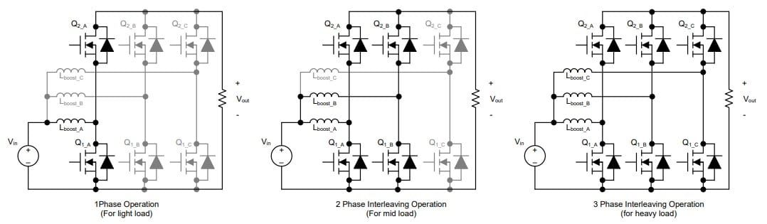 Phase shedding options on TTPL PFC (click on image to enlarge)
In each of these modes the phase shift between each of them must be adjusted. When in two-phase mode, a 180° phase shift is desired between the pulse-width modulators, and when in three-phase mode, a 120° of phase shift is desired.
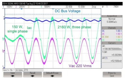
The decision to do phase shedding can be made on different parameters, such as the RMS current, power, the peak inductor current, and so on. When using RMS current the change of phases can be significantly delayed. The following figure shows phase shedding when the decision is based on RMS current. Code takes multiple AC cycles before the phases are added.
 Waveform when decision to add phases is based on RMS calculation.
This delay may not be acceptable for many applications. Thus, the voltage controller output is chosen as the decision point to drop or add phases. A state machine is constructed as shown in the figure below, with some hysteresis built around the phase shedding points.
 State machine for phase shedding control (click on image to enlarge)
Key Components Used in This Reference Design
- LMG3410 GaN Power Stage
The LMG3410 single-channel GaN power stage contains a 70-mΩ, 600-V GaN power transistor and specialized driver in an 8-mm × 8-mm QFN package. Direct drive architecture is used to create a normally-off device while providing the native switching performance of the GaN power transistor.
When the LMG3410 is unpowered, an integrated low-voltage silicon MOSFET turns the GaN device off through its source. In normal operation, the low-voltage silicon MOSFET is held on continuously while the GaN device is gated directly from an internally-generated negative voltage supply.
The integrated driver provides additional protection and convenience features. Fast overcurrent, overtemperature, and undervoltage lockout (UVLO) protections help create a fail-safe system. The device's status is indicated by the FAULT output. An internal 5-V low-dropout regulator can provide up to 5 mA to supply external signal isolators.
Finally, externally-adjustable slew rate and a low-inductance QFN package minimize switching loss, drain ringing, and electrical noise generation.
- UCC27712 600-V High-Side Gate Driver
The UCC27714 used in this design is a 600-V high-side, low-side gate driver with 4-A source and 4-A sink current capability that is targeted to drive power MOSFETs or IGBTs. The device comprises of one ground-referenced channel (LO) and one floating channel (HO), which is designed for operating with bootstrap supplies.
The device features excellent robustness and noise immunity with capability to maintain operational logic at negative voltages of up to -8Vdc on HS pin (at VDD = 12 V).
- C2000™ MCU F28004x for Real-Time Control
C2000 MCUs are part of an optimized MCU family for real-time control application. Fast and high-quality analog-to-digital controller enables accurate measurement of the current and voltage signals, and an integrated comparator subsystem (CMPSS) provides protection for overcurrent and overvoltage without use of any external devices. The optimized CPU core enables fast execution of control loop.
Trigonometric operations are accelerated using the on-chip trigonometric math unit (TMU). The solution also provides an option to use the control law accelerator (CLA) on the F28004x and F2837x. The CLA is a co-processor that can be used to alleviate CPU burden and enable faster-running loops or more functions on the C2000 MCU.