Facebook
 Google
 GitHub
 Linkedin
Designing a 20W Universal-Input LED Driver – New Application Note
Application note AND9714/D from ON Semiconductor describes the key steps to design a LED driver controlled by the NCL30386/88. It provides insights on component selection to obtain a good constant-voltage and constant-current regulation.
The process is illustrated by a practical 20W, universal mains (90- to 265-Vac input) application with an output voltage range of 20- to 40-Vdc and an output current of 500mA
The NCL30386 and NCL30388 are power factor corrected controllers with primary side constant voltage (CV) and constant current (CC) control suitable for flyback, buck-boost or SEPIC. The NCL30386 is housed in an SOIC 10 package and provides analog dimming of the output current with two dedicated dimming control input pins ADIM and PDIM. The NCL30388 is housed in an SOIC 8 package and targets high-performance LED drivers.
These controllers integrate a proprietary circuit for power factor correction and constant current control allowing achieving a power factor above 0.95 with a total harmonic distortion below 10% for universal mains input. The output current and the output voltage regulation are typically within ±2% for an input voltage varying from 85Vac to 265Vac.
The current-mode, quasi-resonant architecture of these controllers optimizes the efficiency by turning on the MOSFET when the drain-source voltage is minimal (valley). The valley lockout and frequency foldback circuitry maintains high-efficiency performance in dimmed conditions or in light load during constant-voltage regulation.
In addition, the circuit contains a set of protections to ensure a robust LED driver design:
- Output Over Voltage Protection
- Cycle-by-cycle Peak Current Limit
- Winding and Output Diode Short Circuit Protection
- Output Short Circuit Protection
- VCC pin Over Voltage Protection
- Floating/Short Pin Detection: the circuit can detect most of these situations which is of great help to pass safety tests
The NCL30386 / 88 offer a board range of options. Among them, there are two selectable reference voltages for the constant current regulation: VREF = 333 mV or VREF = 250 mV. The reference voltage selection directly sets the duty-ratio limit. For VREF = 333 mV, the duty-ratio is limited to 70% at the top of the lowest line sinusoid. For VREF = 250 mV, the duty-ratio is limited to 80% at the top of the lowest line sinusoid.
 Idealized Waveforms of a Flyback Converter in DCM (click on image to enlarge)
In primary-side constant-voltage regulation, the output voltage is sensed via the auxiliary winding. Indeed, the auxiliary winding provides an image of the output voltage during the off-time of the power MOSFET. By sampling the auxiliary voltage knee (which represents the end of the core demagnetization) the controller is able to accurately control the output voltage. Figure 1 illustrates the idealized waveforms of a flyback converter operated in discontinuous conduction mode (DCM). When the secondary current becomes null, the auxiliary winding voltage is sampled on ZCD pin.
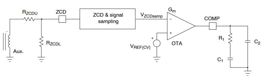 Constant Voltage Feedback Circuit (click on image to enlarge)
The power factor correction operation induces larges variations of the MOSFET off-time. Particularly around the input voltage zero crossing, the demagnetization time is very small and the auxiliary winding voltage cannot be sampled correctly. For this reason, the sampling is disabled whenever the input sine waveform is below 50V with a 5V hysteresis.
In the same way, the sampling is disabled during the ZCD blanking to avoid false reading output voltage caused by the leakage inductance at the power switch turn off. Thus, the power supply designer must ensure that tdemag > 2 s when Vin is above 55V for heavy to medium output load and tdemag > 1.3 s for light load conditions.
In order to select the right components for the loop, it is necessary to find the worst-case operating point for the FB loop. The Bode plot below shows the control to output stage bode plots at maximum output load and at light load. The control to output transfer function is the auxiliary winding voltage divided by the COMP pin voltage since this is a primary side regulated system.
 Bode Plots of the Converter at Maximum Output Load and Light Load (click on image to enlarge)
Because of the control algorithm, the power stage gain increases at light load and the low-frequency pole moves towards lower frequencies. Looking at the phase, the shift is less important at heavy load (-70° versus -90° at light load for the 20-W design example). If the design does not account for this phase shift at light load and considers only the phase at maximum output load to calculate the compensator, this could result in instabilities at light load.
On another hand, if the design calculates the compensator based only on the light load transfer function, the loop bandwidth would be very limited. For this design, it can be seen that, based on the light-load curves, the chosen crossover frequency could not be higher than 8Hz because the power stage phase shift is already -90° at 8Hz and the type compensator can only bring a phase boost up to 90°.
Thus, compensating at light load only results in low bandwidth and sluggish transient output load response. A specific compensation method is proposed to avoid this situation.
Conclusion
This application note shows the steps to design a LED driver controlled by the NCL30386 and the NCL30388. This new family of controllers provides a very good regulation of the output current / voltage from the primary side of a flyback controller while maintaining a good power factor with low total harmonic distortion.