Facebook
 Google
 GitHub
 Linkedin
200V and 650V Enhancement-Mode GaN Devices on 8” Wafers
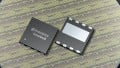
Imec has developed 200V and 650V normally-off/enhancement mode (e-mode) on 200mm/8-inch GaN-on-Silicon wafers, achieving a very low dynamic Ron dispersion (below 20 percent) and state-of-the-art performance and reproducibility. Stress tests have also shown a good device reliability. Imec's technology is ready for prototyping, customized low-volume production as well as for technology transfer.
GaN technology offers faster switching power devices with higher breakdown voltage and lower on-resistance than silicon, making it an ideal material for advanced power electronic components. Imec’s GaN-on-Si device technology is Au-free and compatible with the wafer handling and contamination requirements for processing in a Si fab. A key component of the GaN device structure is the buffer layer, which is required to accommodate the large difference in lattice parameters and thermal expansion coefficient between the AlGaN/GaN materials system and the Si substrate.
Imec achieved a breakthrough development in the buffer design (patent pending), allowing to grow buffers qualified for 650 Volt on large diameter 200mm wafers. This, in combination with the choice of the Si substrate thickness and doping increased the GaN substrate yield on 200mm to competitive levels, enabling low-cost production of GaN power devices.
Also, the cleaning and dielectric deposition conditions have been optimized, and the field plate design (a common technique for achieving performance improvement) has been extensively studied. As a result, the devices exhibit dynamic Ron dispersion below 20% up till 650 Volt over the full temperature range from 25 to 150 degrees C. This means that there is almost no change in the transistor on-state after switching from the off-state, a challenge typical for GaN technology.
“Having pioneered the development of GaN-on-Si power device technology on large diameter substrates (200mm/8-inch), imec now offers companies access to its normally-off/e-mode GaN power device technology through prototyping, low-volume manufacturing as well as via a full technology transfer†stated Stefaan Decoutere, program director for GaN technology at imec.
“Next to enhancement mode power device switches, imec also provides lateral Schottky diodes for power switching applications. Based on imec’s proprietary device architecture, the diode combines low turn-on voltage with low leakage current, up to 650V – a combination that is very challenging to achieve,†Decoutere concluded.