Facebook
 Google
 GitHub
 Linkedin
UnitedSiC Unveils Four JBS Diodes, Augmenting its Schottky Diode Portfolio
The new 1200 and 1700 volt Junction Barrier Schottky (JBS) diodes join the company’s 3rd generation of silicon carbide MPS diodes.
Defining a figure of merit (FoM) as VF times Qc, United SiC claims a 12 to 15% lead over the rest of the industry. The new units are aimed at highly efficient power system designs employing the highest switching speeds.

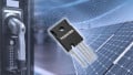
Image courtesy of UnitedSiC
The new SiC Merged PiN-Schottky (MPS) diodes feature zero reverse recovery charge and maximum junction temperatures of 175°C. When dealing with high currents, the PN junction enables the injection of more charge carriers, allowing the units to withstand up to 12 times the rated current. All units feature no reverse or forward recovery and are capable of being parallel.
The Difference Between a Schottky Diode and a JBS Diode?
A Schottky Diode is formed by the junction of N-type semiconductor material with metal. The metal acts as the anode while the N-type semiconductor forms the cathode. These devices are characterized by low voltage drops and fast switching.
The more familiar PN Diode generally can’t switch as quickly, but they enjoy higher reverse voltage ratings
Silicon Carbide (SiC) diodes, as described by UnitedSIC, are “are majority carrier devices and have no minority carriers injected into and stored in the drift layer during normal forward operation. Therefore, unlike Si PiN diodes, SiC JBS diodes have no stored charge or stored charge related reverse recovery time and can be turned off much faster.”
As Anup Bhalla, VP Engineering at UnitedSiC, explains: “Through the unique characteristics of the UJ3D1725K2, we can provide our customers with reliable, space-saving, cost-effective SiC diodes that have substantially better performance levels and assured quality, supported by high volume manufacturing.”

The UJ3D1725K2. Image courtesy of UnitedSiC Data
The New Models
- UJ3D1725K2 1700 volts at 25 Amps
- UJ3D1210K2 1200 Volts at 10 Amps
- UJ3D1220K2 1200 Volts at 20 Amps
- UJ3D1250K2 1200 Volts at 50 Amps
SiliconSiC provides a guide to the members of UJ3D series. From there, it easy to find other information, including the datasheets for all the devices
Important Features
VR, VRRM and VRSM
- For the UJ3D1725K2, these parameters are all specced at 1700 volts.
- For the UJ3D1210K2, UJ3D1225K2, and the UJ3D1250K2, the corresponding figure is 1200 volts
Power Dissipation
- UJ3D1725K2: 283 watts and 69.8 watts at TC equal to 25℃ and 138℃, respectively
- UJ3D1210K2: 136.4 watts and 26.4 watts at TC equal to 25℃ and 146℃, respectively
- UJ3D1220K2: 205 watts and 55 watts at TC equal to 25℃ and 135℃, respectively
- UJ3D1250K2: 319 watts and 134 watts at TC equal to 25℃ and 112℃, respectively
Thermal Resistance, Junction to case
- UJ3D1725K2: 0.41 (typ) ℃/W
- UJ3D1210K2: 0.83 (typ) ℃/W
- UJ3D1220K2: 0.56 (typ) ℃/W
- UJ3D1250K2: 0.36 (typ) ℃/W
Total Capacitance Charge (QC)
This figure actually depends on multiple factors. Designers would do well to consult datasheets. The typical figures below assume, for a start, VRs of 800 volts for the UJ3D1210K2, UJ3D1220K2, and the UJ3D1250K2 and VRs of 1200 volts for the UJ3D1725K2
- UJ3D1725K2: 184 nC
- UJ3D1210K2: 51 nC
- UJ3D1220K2: 83 nC
- UJ3D1250K2: 240 nC
Applications
- Fast-charge electric vehicle (EV) charging
- Industrial motor drives
- Solar energy inverters
- Power converters
- Switch-mode power supplies
- Power factor correction module
Physical and Regulatory Considerations
The new devices are compliant with the AEC-Q101
They are available in die form and in TO247-2L packages.