Facebook
 Google
 GitHub
 Linkedin
Toshiba Sampling Industry’s Lowest ON Resistance Load Switch ICs
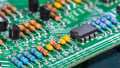
Toshiba America Electronic Components, Inc. (TAEC) has started shipping samples of three new ultra-low-voltage load switch ICs that claim the industry's smallest switch ON resistance. The TCK206G, TCK207G and TCK208G join Toshiba's broad lineup of load switch ICs for mobile devices. With an embedded reverse current block (RCB) circuit and a slew rate control driver, the TCK206G, TCK207G and TCK208G are designed for use as a power management switch IC in smartphones, tablets, ultrabooks, and other mobile equipment. The new products feature very-low ON resistance and very-low input operating voltage, in an ultra-compact package, which was achieved using Toshiba's newly developed CMOS process and unique analog circuit design techniques.
As mobile devices trend towards higher battery capacity--and become smaller and lighter--there is an increased demand for ultra-compact, low power consumption, low power dissipation switches. Available in a 0.5mm pitch WCSP4C package, the TCK206G, TCK207G and TCK208G are suited for portable applications that require high-density board assembly. Key features include: Low input voltage operation: V(IN) = 0.75 to 3.6V; Low ON resistance, R(ON) = 18.1m ohms (typ.) @V(IN) = 3.3V, I(OUT) = -1.5A; R(ON) = 18.2m ohms (typ.) @V(IN) = 1.2V, I(OUT) = -1.5AR(ON) = 18.4m ohms (typ.) @V(IN) = 0.75V, I(OUT) = -1.5A; Inrush current is limited by the slew rate control driver; Reverse current blocking; Built in Auto-discharge (TCK207G and TCK208G); Ultra small package: WCSP4C (0.9mm×0.9mm, t: 0.5mm(typ.))
The TCK206G, TCK207G and TCK208G are now sampling. All three devices include inrush current limiting and reverse current blocking. Output auto-discharge is included with the TCK207G and TCK208G and is not available on the TCK206G. The control pins are pull down, active high on the TCK206G and TCK207G and Open, active low on the TCK 208G. Budgetary pricing begins at $0.10, with volume discounts available.