Facebook
 Google
 GitHub
 Linkedin
The Spinout Behind the Next Generation Miniature Power Converters
With the recent advancements in consumer and industrial electronics that aim for added performance and functions in small size comes a great demand for novel power converter technologies that can cope with such a trend.
Faster speeds and more functions require more power. However, product design and user experience demands put strict limitations on increasing the platform size. That translates to a need to process more power in the same space, or otherwise the same power in less space. In technical terms, that translates to higher power densities.
In a battery-operated device, there exists a single source of power. That is either the battery (most common is the lithium-ion technology) or the adapter when docked (USB is most common). That source offers a specific terminal voltage that can vary across the operational cycle (e.g. battery terminal voltage depending on the state of charge). On the other hand, the platform hosts various loads including the chipset, sensors, and other system bill of material components. Those loads operate at different voltages, and each may feature a number of power states, each requiring a specific supply voltage. On top of the electrical characteristics of voltage and current, additional specifications are placed in applications with specific operational requirements. For example, the analog and RF chipset require very low noise on the supply, while the digital processor core dictates fast transient response as well as configurable supply voltage according to clock speed (e.g. Voltage ID).

Figure 1. Lotus Microsystem’s Miniature 5 V Step-Down Converter. Image used courtesy of Bodo’s Power Systems [PDF]
The platform power management and delivery system is responsible for the translation of the single input power rail to the variety of rails needed by the platform chipset and other loads. It is comprised of an array of power converters that are mostly powered from the same source, yet deliver different electrical characteristics for different loads. On a modern smartphone, 15-20 different rails are needed to be supported by the power delivery system, which makes its design and implementation process a challenging task, especially when engineers are faced with strict limitation on the system footprint and profile (weight is also of significance in applications like wearables and drones).
The current technologies for power converters are hardly coping with such trend for increased power densities. Large footprint is taken up for the power delivery system, which in some cases amount to about one third of the platform area. The reduction of such system size can be utilized towards additional chips on the platform (more functions) or otherwise space for a bigger battery (longer use time). However, attempting at the reduction of such system size by using absolute minimum margins and clearances between components leads to thermal issues that result in higher operating temperatures. In some cases, high power loss congestion can result in hotspots that exceed the thermal roof of the device, and can lead to catastrophic effects if the battery is not well-isolated. Another issue of operating at high temperatures is the increased parasitic effects that result in higher losses and less use time for the battery charge. From a sustainability angle, the current manufacturing technologies rely on the extensive use of raw materials that, when scaled over billions of devices, result in environmental consequences. In addition, the requirement for expensive and eco-unfriendly cooling structures needed to take the heat out of the power delivery system (e.g. in datacenters) creates a huge carbon footprint.

Figure 2. Lotus Microsystem’s LMS1206 device offers the best-in-class power (W) per mm3. Image used courtesy of Bodo’s Power Systems [PDF]
Lotus Microsystem’s value proposition addresses the challenges above. By using a silicon substrate for the power converter, we have developed substantially smaller and lighter power electronics that can cope with today’s trend for more functions in small sizes. That comes without sparing the thermal performance of the power converter. Further, silicon is a naturally abundant resource that is simple to process and allows for great savings in the manufacturing material.
The technology behind is the Lotus Microsystems’ patented Power Interposer Technology (PIT). We start with a silicon wafer that we process in such a way that allows us to create customized silicon structures with circuits and interconnects using a set of features that include double-sided wafer routing, precise copper etching, high-aspect ratio through-silicon vias (TSVs), in addition to precise silicon etching. Furthermore, the entire flow is CMOS compatible.

Figure 3. Superior Thermal Performance compared to a replica PCB based module. Image used courtesy of Bodo’s Power Systems [PDF]
That results in three main unique selling points (USPs) for our technology. The first being the best-in-class power density, which comes from embedding the active or passive power converter components in the substrate and results in substantial reduction of the converter footprint and/or profile. The second is the superior thermal performance, thanks to the higher thermal conductivity of the silicon material compared to the different variants of the FR4 material in state-of-the-art PCB technology. The third is the scalability of electrical characteristics with respect to voltage and current capabilities, where higher voltages are enabled through thicker layers of passivation, while higher currents come from thicker copper layers and TSV structures. That opens for the employment of our patented technology in a wide range of applications, and we have demonstrated solutions for the bus voltages of 5 V and 12 V.
Lotus Microsystems was founded in 2020 by three PhD graduates from the Technical University of Denmark. The research behind started five years earlier and the founding team received a series of support grants to mature the technology and analyze the commercial potential prior to spinning out. Since the foundation, the company received several endorsements from Danish and European support schemes and closed two rounds of investments.
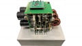
Currently, the company is getting ready for the launch of two products. The first is the LMS1206 device, which is a compact 36 W converter based on the proprietary silicon substrate technology. The converter offers superior thermal stability and high efficiency in a compact 6.2 mm x 6.7 mm footprint, and a profile of 2.5 mm. The power module integrates the power devices, controller, compensation network, as well as the magnetic devices, with a set of industrial protection features such as OCP, OVP, SCP, and OTP.

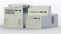
Figure 4. Evaluation boards are ready for sampling. Image used courtesy of Bodo’s Power Systems [PDF]
It is a standard component that targets a set of applications including mobile devices, PCI industrial applications, telecom devices, and others. Next in the stack is the LMS501XC device, which targets applications powered from a single Li+ cell, such as wearables and IoT sensors. The module integrates the power devices, control IC, and inductor in a compact 2.6 mm x 2.0 mm and a profile of 2 mm. Both products are currently available for sampling along with the products’ documentation.
This article originally appeared in Bodo’s Power Systems [PDF] magazine.