Facebook
 Google
 GitHub
 Linkedin
System Benefits of Using G1 Series Intelligent Power Modules (IPM)
This article discusses the system benefits and advantages of using Mitsubishi Electric's G1 Series Intelligent Power Modules for inverter designs.
Mitsubishi Electric integrates several key technologies into one power module in order to deliver the best possible overall system performance. The G1 IPM concept addresses three areas crucial for inverter designers – Easy design, High efficiency and High reliability.
Easy design: The G1 IPM is provided with an internal gate drive unit, multiple integrated protection functions and a failure output signal for easy facilitation of failure recognition. The incorporation of these functions into the G1 IPM relieve the inverter designers from extensive verification tests as all functions are fine-tuned to the built-in 7th gen IGBT/FWDi-chipset and which are 100% tested by the module manufacturer. Another feature going in favor of the design process is the busbar design flexibility option: the ‘A’ package variant (refer Figure 2) offers two possible main terminal positions. One option is where the AC output side is placed in parallel with the DC input terminal and another option is where the DC input terminal is placed at a 90° angle to the AC output terminal (with both variants available in either screw-type terminal or solder-type terminal).
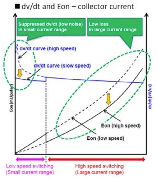
Figure 1: dv/dt and Eon control in G1 IPM
High efficiency: The IGBT chip is based on a special internal gate design optimized for the IPM’s ‘short circuit capability versus losses’ trade-off, and as a result the ON state loss behavior is significantly lower than a conventional IGBT device and the Vcesat versus Eoff characteristic is also superior in comparison with a conventional IGBT device. In combination with this special gate design, this improved IGBT chip is provided with a monolithically integrated current mirror to implement a current sensing scheme. There are two main benefits offered by such a current sensing scheme. Firstly, an effective SC protection can be realized which is based on the instantaneous device current Ic. The trip level of such an SC-protection can be established independent of the IGBT-desaturation, thus being much faster than the conventional desat-protection. Secondly, an innovative switching speed control can be established depending on the actual value of the device current Ic. This means - a reduced speed (for Low EMI) turnon at low Ic values and a high-speed turn-on (low turn-on loss) at high Ic values can be achieved (refer Figure 1). These key features ensure a significantly higher inverter efficiency and good EMI performance.
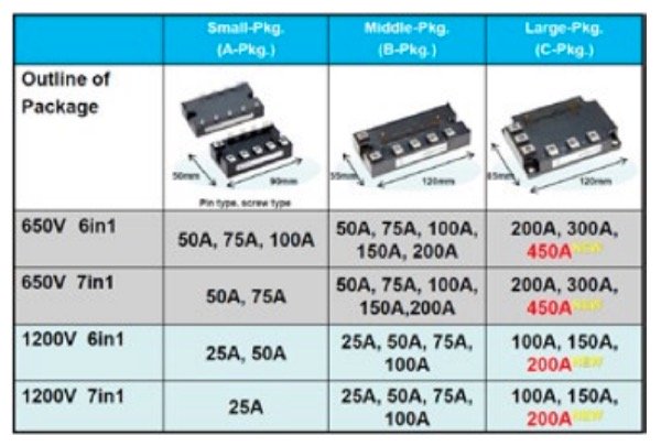
Figure 2: Line-up of the G1 IPM modules
High reliability: The module packaging design and chip design have been established with ‘product reliability’ assuming the utmost importance. The module consists of built-in functions which aid in failure detection, module’s self-protection activation and facilitates failure type recognition. An important feature is that the IGBT is provided with an on-chip temperature sensor to detect an over-temperature directly in the silicon. There is a power supply under-voltage protection system and an innovative short-circuit protection scheme. The G1 module packaging technology aims to improve the withstand capability against stress factors causing degradation/aging of the module. The module employs the SLC (Solid Cover) technology along with an innovative IMB (Insulated Metal Baseplate) structure. As a result, the module exhibits superior thermal cycling behavior while providing lower thermal resistance.
About Mitsubishi Electric
Mitsubishi Electric is one of the world’s leading companies in Manufacturing, Marketing and Sales of electric and electronic equipment used in communications, industrial technology, renewable energy and transportation.
This article originally appeared in the Bodo’s Power Systems magazine.