Facebook
 Google
 GitHub
 Linkedin
STMicroelectronics Releases Two Series of MDmesh Silicon Power MOSFETs
ST’s STPOWER MDmesh M9 and DM9 series feature N-channel super-junction multi-drain silicon power MOSFETs that will offer what ST says are the best RDS(ON)s in their categories.
Introduced early last week at PCIM Europe 2022, the 600 V STP60N043DM9 and 650 V STP65N045M9 are the first members of the MDmesh DM9 and M9 series, respectively. Both devices feature low RDS(ON)s per unit area, maximizing power density and saving precious board space, in addition to typical gate charges (Qg) of only 80 nC.

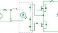
The STP60N043DM9 and STP65N045M9. Screenshot used courtesy of STMicroelectronics
With maximum RDS(ON)s of 45 mΩ for the STP65N045M9 and 43 mΩ for the STP60N043DM9, ST claims the fresh offerings sport best-in-class RDS(on)max x Qg figures of merit (FoM).
More Key Advantages
Gate threshold voltages of 3.7 V for the STP65N045M9 and 4 V for STP60N043DM9 serve to minimize both turn-on and turn-off switching losses when compared to members of the earlier MDmesh M5, M6 and DM6 series. The two new devices also offer decidedly low reverse recovery times (trr) and reverse recovery charges (Qrr), serving to further improve the devices’ switching performances and efficiencies, STMicroelectronics said in its release.
What’s more, these first units feature — as will subsequent members of the MDmesh M9 and DM9 series — an additional platinum diffusion process that ensures a fast intrinsic body diode. There is as well an improved peak diode-recovery slope (dv/dt) and, at 400 V, the fresh offerings can withstand dv/dt rates of up to 120 V/ns.
Absolute Maximums
For both the STP65N045M9 and the STP60N043DM9:
- Rated at maximum G-S voltages of ±30 V
- MOSFET dv/dt ruggedness is specced at 120 V/nS
- Total Power dissipation is 245 W
STP60N043DM9, specific:
- Continuous Drain Current: 56 A
- Pulsed Drain Current: 175 A
STP65N045M9, specific:
- Continuous Drain Current: 55 A
- Pulsed Drain Current: 170 A
Thermal Data
For both devices:
- Thermal resistance, junction-to-case: 0.51 °C/W
- Thermal resistance, junction-to-ambient: 62.5 °C/W
On and Off States
Both units offer:
- Zero gate voltage drain current at the individual device’s maximum drain-source voltage: 200 μA
- Gate to body leakage current: ±100 nA
Dynamic Characteristics
For the STP60N043DM9, dynamic characteristics are as follows:

STP60N043DM9 — Dynamic Characteristics. Screenshot used courtesy of STMicroelectronics
And for the STP65N045M9:

STP65N045M9 — Dynamic Characteristics. Screenshot used courtesy of STMicroelectronics
Switching Times
For the STP60N043DM9, switching time characteristics are as follows:

STP60N043DM9 — Switching Time Characteristics. Screenshot used courtesy of STMicroelectronics
And for the STP65N045M9:

STP65N045M9 — Switching Time Characteristics. Screenshot used courtesy of STMicroelectronics
Applications
- High efficiency switching power supplies (SMPS)
- LLC resonant converters
- Data-center servers
- 5G infrastructure
- Flat-panel televisions
Physical Considerations
- These MDmesh Silicon Power MOSFETS operate over a junction temperature range of -55 to 150 ℃
- The devices are available in TO-220 packages