Facebook
 Google
 GitHub
 Linkedin
STMicro Debuts Op Amp With Unity-Gain-Stability and a 22MHz Gain Bandwidth Product
The new device features a slew rate of 11 volts/µsecond and a maximum input-offset of 200 µvolts
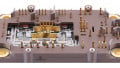
The TSV7722 from STMicroelectronics is a two-channel op amp targeting energy efficient power conversion, suitable for current measurement and high-speed signal conditioning.

The TSV7722. Image courtesy of ST
The TSV7722 features a typical input offset voltage of 50µV at 25°C and an input-voltage noise density of 7nV/√Hz, enabling accurate low-side current measurements. The input bias current of 2pA (typ) allows for solid photodiode-current measurement, important to optical-sensing applications including smoke detectors.
The TSV7722 meets its stated specifications while serving an output capacitive load of 47 pF, enabling the unity gain stable device to serve well as an ADC input buffer.
The TSV7722 is a low rail input, rail-to-rail output device. The unit operates from any power supply over a range of 1.8 to 5.5 volts and typically consumes 1.7 mA per channel at 5 volts.
The TSV7722 is included in ST’s 10-year longevity program, which will serve to assure OEMs that the unit will be available for at least 10 years into the future.
The TSV7722 targets Energy Efficient Power Conversion
The op amp features gain-bandwidth of 22MHz and slew rate of 11V/μs, as described. And, through its speedy and highly accurate current measurements, ST’s new op amp facilitates the quick responses to real-world changes that are imperative to the efficient conversion of power.
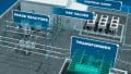
The unit is actually optimized for low-side current sensing. This method is affected by inserting a sense resistor between the load and ground.

Low side current sensing with the TSV7722. Image courtesy of datasheet
The voltage drop across the shunt is measured by the op amp, and the current can thereby be deduced.
Absolute Maximums
- Power supply (VCC) maximum is 6 volts
- Differential input voltage is ±VCC
- Input pins input current ± 10 mA
- Thermal resistances, junction to ambient (Rth-ja) are 127 ℃/watt and 76 ℃/watt for MiniSO8 and DFN8 packages, respectively
Electrical Characteristics
These values are for VCC at 5 volts and the datasheet provides complete information. However, ST states that these parameters are very stable over the full VCC range.
- Input offset voltage drift is ±4 μV/°C when the common-mode voltage is zero
- Input offset current (with VOUT = VCC/2) is 1 pA at 25℃, and over the device’s operating temperature range it’s typically under 20 pA
- Unity gain frequency, with a 47 pF load, is 19.5 MHz (typ)
- Overload recovery time 70 ns
- Settling time is 270 ns
- Channel separation @ 1kHz is 120dB
- Differential and common mode input capacitances are 6 pF and 4.5 pF, respectively
Applications
- Automotive applications including current measurement and sensor signal conditioning
- Solar panels
- Telecom infrastructure
- Servers
- Signal conditioning for strain gauges
- Low-side current measurement
- Photodiode amplifiers
Physical Concerns
- The TSV7722 is currently available in MiniSO8 and DFN8 packages
- The unit operates over a -40 to +125℃
Safety and Regulatory
ESD protection:
- 4 kV human body model (HBM)
- 1.5 kV charged device model (CDM)
ST notes that automotive qualified versions of the TSV7722 will be available in the second half of 2021.