Facebook
 Google
 GitHub
 Linkedin
Safer Linear Mode Operation with Wide SOA MOSFETs
STMicroelectronics has introduced a 100V power MOSFET manufactured with advanced STPOWER STripFET F7 technology and housed in an H2PAK package. The device is designed for rugged operations with forward bias safe operating area (FBSOA), where high power levels are required in the event of high drain-source voltage (VDS) drops [1].
The new STH200N10WF7-2 power MOSFET is suitable for industrial and motor drive applications and can be used for linear motor controllers and inrush current limiters, where the current flow is set by tuning the gate-source voltage (VGS) of the MOSFET and high capacitive loads require a heavy charge phase at constant current.
The device is able to provide high immunity to the thermal runaway better than advanced planar devices under linear mode working conditions. The wide SOA capability is the result of the optimization of the STPOWER STripFET F7 technology in terms of setting the gate-source voltage (VGS) to obtain modulated threshold voltage (Vth) and transconductance (Gfs) values for the device [2]. In this way, the MOSFET becomes more robust in linear mode and thermally stable for a wider range of operating conditions in the safe operating area (SOA).
The STH200N10WF7-2 for Linear Motor Control
The wide SOA MOSFET (STH200N10WF7-2) offers excellent performance in linear motor control systems, such as the fan control. The HVAC (Heat Ventilation Air Conditioning) system can usually be accomplished according to the block diagram shown in Figure 1.

Figure 1. Block diagram of a linear motor control system. Image used courtesy of Bodo’s Power Systems
The gate-source voltage (VGS) of the MOSFET can be changed by adjusting the duty cycle of the bipolar transistor, so it is possible to change the current through the motor and its speed. The current is set by the equivalent resistance provided by the MOSFET, when biased under FBSOA working conditions. In this case, the STH200N10WF7-2 has to withstand a very stressful condition as high power levels are required with a high drain-source voltage (VDS) drop. The waveforms measured in steady state working conditions are shown in Figure 2.
The above figure shows the main signals of the power MOSFET when the application works at a fixed operation point. The green trace represents the current flowing through the motor and then the MOSFET with an average value of about 6.5A. The red trace is the drain-source voltage drop across the MOSFET and the dark blue curve is the gate-source voltage that drives the device. A low gate source voltage value just above the MOSFET threshold allows the setting of the equivalent resistance which is connected in series to the motor. In this way, the amount of current flowing through the motor is defined and the motor speed regulated. The dark green trace represents the power dissipation in the device defined as the product of the drain source voltage drop and the current.
Additional measured waveforms showing the power dissipation at start-up when the duty cycle is set at 50% are reported in Figure 3.

Figure 2. Measured waveforms in steady state conditions. Image used courtesy of Bodo’s Power Systems

Figure 3. Measured waveforms at start-up. Image used courtesy of Bodo’s Power Systems
Due to the stalled condition of the motor at start-up, the peak inrush current reaches nearly 18A. This peak is related to the back EMF (Electro-Magnetic Force) that, for a DC brushed motor, is zero when the motor is not running. This transient condition implies a temporary inductive short circuit used to overcome the mechanical inertia. Once the motor starts running, the current returns to the steady state condition with a much lower average value. The maximum power dissipation at start-up is about 110W, as shown by the dark blue trace in the above figure.
The STH200N10WF7-2 MOSFET
The wide SOA MOSFET can achieve much better thermal stability in linear mode operation than the standard trench device and assure quite a self-balanced current, as shown in Figure 4.
The simulated drain current curves over time for ST’s standard and wide SOA device show excellent stability for the STH200N10WF7-2.
This feature makes this device suitable for linear controller fan motor applications. In fact, due to the flat output current with respect to the VDS voltage (as shown in Figure 5) at DC operating condition is easier to manage the tuning of the VGS and ID for protecting the system from unwanted thermal instability and device failures.

Figure 4. Simulated drain current stability over time. Image used courtesy of Bodo’s Power Systems

Figure 5. Output characteristics of the STH200N10WF7-2 (at different temperatures). Image used courtesy of Bodo’s Power Systems
The key parameter to select the proper MOSFET for linear mode motor control application is then the thermal coefficient of the drain current (TC) [1]:
\[TC=\frac{aI_{D}}{aT}\]
which defines the power capability and relevant stability of a MOSFET working in linear mode, as shown by the following equation:
\[TC=\frac{aI_{D}}{aT}\Big|_{I_{D}=const} = \frac{1}{V_{DS}\cdot R_{thJA}}\]
The external application conditions determine the VDS voltage drop and the junction-ambient thermal resistance (RthJA) of the system while the thermal coefficient is intrinsic to the device technology. The condition of equilibrium defined in the above equation (2) establishes the boundary condition to trigger the thermal instability [3].

Figure 6. Thermal coefficient of the wide SOA STH200N10WF7-2 at different VDS. Image used courtesy of Bodo’s Power Systems
To be effective and robust under FBSOA permanent working conditions, the MOSFET has to exhibit a thermal coefficient with a small peak and a rather narrow range of positive values (Figure 6) [2].
The new device can even exceed the performance of advanced planar MOSFETs in linear mode operation due to its thermal stability for a wider range of operating conditions within the SOA, as illustrated in Figures 7, 8.

Figure 7. Measured and theoretical curves for an advanced planar device. Image used courtesy of Bodo’s Power Systems

Figure 8. Measured and theoretical curves for the wide SOA device. Image used courtesy of Bodo’s Power Systems
The green curves represent the real SOA measured on an advanced planar MOSFET and the wide SOA device. For the wide SOA MOSFET, the experimental data show that the measured curve is closer to the theoretical curve (red trace) for a wider voltage range [3].
As a consequence, the new advanced trench device is able to withstand the linear mode operation up to 25V, while the advanced planar device starts to trigger the instability region for VDS > 15V. The relevant thermal pictures at VDS = 15V (for planar device) and VDS = 25V (for wide SOA device) are shown in Figure 9.

Figure 9. Thermal pictures for the planar device @ VDS = 15V (left) and wide SOA device @ VDS = 25V (right). Image used courtesy of Bodo’s Power Systems
The thermal picture shows how in linear mode operation the active area of the wide SOA MOSFET involved in managing the power dissipation is reduced at higher VDS voltage drops and is concentrated in a limited hotter area only.
Measured Linear Mode Performance
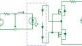
The linear mode ruggedness of the STH200N10WF7-2 was experimentally verified and compared with a standard trench technology MOSFET using the test circuit shown in Figure 10.
Turning on the controller MOSFET, the source pin of the D.U.T. goes to ground, therefore the bias voltage provided by Vcc is fully applied to the drain of the D.U.T. The Zener diode (Dz) clamps the voltage at its limit value and allows a current flowing through R1. The voltage drop on R1 turns on the D.U.T. in linear mode. The C capacitor provides an extra current capability to the power supply in order to feed the circuit during the power pulse.
The following test conditions have been considered:
Vcc = 40 V – 44 V
RG = 47 kΩ
C = 2 x 47000 µF.

Figure 10. Testing circuit for linear mode ruggedness. Image used courtesy of Bodo’s Power Systems
The external RG resistor connected to the gate is used to slow down the fast-rising edge of the current when the MOSFET is turned on and, by doing so, the maximum current capability of the MOSFET can be increased [3].
The measured waveforms relevant to the standard and wide SOA devices just before failure are shown in Figure 11.

Figure 11. Measured waveforms for the standard and wide SOA device. Image used courtesy of Bodo’s Power Systems
The standard trench device exhibits much lower current capability than the relevant wide SOA solution with the same die size and thermal resistance. In fact, the standard trench device fails with a 10ms pulse when the drain current reaches 4.3A, whereas the new wide SOA MOSFET can properly work under the same conditions with a current up to 27.6A.
The above reported bench measurements at both application and device levels to verify the linear mode ruggedness demonstrate that the STH200N10WF7-2 is robust under DC FBSOA working conditions and therefore suitable for linear mode motor control applications.
This article originally appeared in Bodo’s Power Systems magazine.