Facebook
 Google
 GitHub
 Linkedin
Infineon Devices Combine GaN Half-Bridge and Gate Drivers
The CoolGaN Drive HB 600 V G5 family packs two GaN switches, high- and low-side drivers, and a bootstrap diode into a single compact module for motor drives and power supplies.
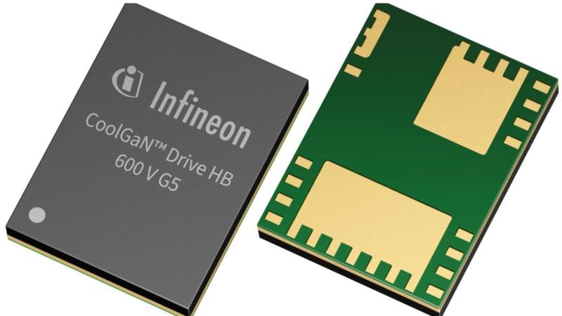
Infineon Technologies has launched the CoolGaN Drive HB 600 V G5 product family, expanding its gallium nitride portfolio with four devices that combine a complete half-bridge power stage into a single 6 x 8 mm package.
The family targets power engineers designing motor drives, switched-mode power supplies, and other compact high-efficiency systems who want to take advantage of GaN's performance without the layout headaches that have historically come with it.
The 600 V 65. Image used courtesy of Infineon
GaN Layout Challenges
GaN transistors switch far faster than conventional silicon MOSFETs, and that speed is both their strength and their complication. Because GaN devices switch so quickly, even small amounts of stray inductance in PCB traces can cause voltage spikes, ringing, and efficiency losses.
Placing discrete gate drivers close enough to the transistors to avoid these effects demands careful, constrained PCB layout work, and the bootstrap circuitry needed to drive the high-side switch adds more components and more routing decisions. That complexity is a real barrier for engineers working with tight board space or compressed development timelines.
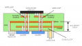
Infineon's approach with the CoolGaN Drive HB 600 V G5 is to remove those decisions from the board-level design entirely. Each device integrates two 600 V CoolGaN G5 transistors in a half-bridge configuration along with high- and low-side gate drivers, a level shifter, and a bootstrap diode, all in a 6x8mm TFLGA-27 package with exposed pads for heat spreading.
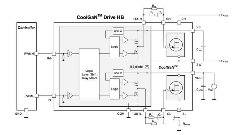
Typical circuit configuration. Image used courtesy of Infineon
The gate driver operates from a single 12 V supply and accepts a standard PWM input compatible with common logic levels, so the interface to a microcontroller or DSP is straightforward. Infineon says the package supports heatsink-less designs in many applications, which further reduces system bulk.
Rated for Various Applications
The four devices, which vary in on-resistance to suit different power levels, achieve a typical propagation delay of 98 ns with low channel mismatch between the high- and low-side switches. Consistent timing between the two switches is important for half-bridge topologies because mismatches can cause timing asymmetry that degrades efficiency or, in worst cases, leads to shoot-through.
The parts also feature zero reverse-recovery charge, a key GaN advantage over silicon that eliminates a significant source of switching loss in bridge circuits.
Designers can adjust the dv/dt switching speed through external resistors, giving them a knob to trade off between switching losses and electromagnetic interference, depending on their application's requirements. Fast under-voltage lockout (UVLO) recovery is included to keep behavior predictable during start-up and supply transients, which is a common pain point in motor drive applications where the supply rail can fluctuate during load steps.
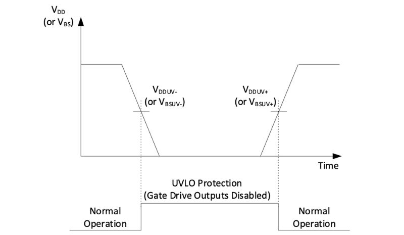
UVLO protection. Image used courtesy of Infineon
The JEDEC-qualified family is rated for applications including motor drives, AC-DC and DC-DC converters, LLC resonant converters, and synchronous buck/boost topologies. Infineon specifically mentions low-power motor drives and switched-mode power supplies as primary targets, and the broader CoolGaN Drive family, including 700 V G5 single switches with integrated drivers in PQFN packages, has been designed for light electric vehicles, portable power tools, and consumer appliances such as fans and vacuum cleaners.
GaN Integration
The CoolGaN Drive HB 600 V G5 is part of Infineon’s wider effort to lower the barrier to GaN adoption. GaN power devices have been commercially available for over a decade, but uptake in the industrial and mid-power consumer segments has been slower than the technology's performance would suggest, largely due to the design expertise required to achieve reliable, efficient results.
Integrating the gate driver alongside the switch—what the industry often calls a GaN power IC or integrated power stage—reduces the number of variables a designer has to manage, and makes GaN behave more like a drop-in upgrade over silicon in familiar topologies.
The devices are availabe through Rutronik.