Facebook
 Google
 GitHub
 Linkedin
Infineon Adds 24 Volt Dual-Channel Low Side Gate Driver to its EiceDRIVER Family
The new driver features dual 10 amp source and sink drive capabilities and an integrated thermal pad to reduce junction to case thermal resistance
The EiceDRIVER 2ED24427N01F features a maximum of 450 mΩ source and sink ON Resistance and 55 ns propagation delays on each of its symmetrical channels. Its built-in thermal pad helps to diffuse heat to the PCB, enabling the driver to handle higher current at high switching speeds.

The EiceDRIVER 2ED24427N01F. Image courtesy of Infineon
The 2ED24427N01F is a low-side non-inverting gate driver for IGBTs, MOSFETs or Infineon modules such as the EasyPACK or EconoPACK. It enables higher power and faster switching frequencies and, because of its highly integrated nature, eliminates multiple associated components and simplifies the design process. The result is a savings in board space and improvements in both reliability and manufacturability
What are Low-Side and High-Side Drivers?
An n-channel driver placed between the load and ground, as on the left, is referred to as a low-side driver.

Low Side and High-Side Drivers. Image courtesy of Electrical Engineering Stack Exchange.
A p-channel driver placed between the load and VDD, as on the right, is referred to as a high-side driver.
Main Features and Benefits of the 2ED24427N01F
The 2ED24427N01F features Infineon’s proprietary latch immune CMOS technology that enables monolithic construction. The device is compatible with standard CMOS or LSTTL outputs of 3.3, 5 or 15 V, and it features a current buffer stage and a high pulse current buffer stage designed for minimum driver cross-conduction. An important consideration is that propagation delays between two channels are matched.
The driver maximum supply voltage is 24 volts, and undervoltage lockout occurs at 11.5 volts

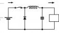
Simplified Application diagram for the 2ED24427N01F. Image courtesy of Infineon
Additionally, the device, with the inclusion of a transformer and other components, can also be used to drive a single high-side FET. The datasheet provides more details.
Because of the device’s high output current and low thermal resistance with respect to the pcb, the 2ED24427N01F can drive even those MOSFETs with very large input capacitance at frequencies of up to 200 kHz or better with no need for a negative voltage supply.
Dynamic Characteristics
- Maximum turn-on and turn-off propagation delays (tON and toff) are 40 and 55 ns, respectively.
- Maximum enable turn-on and turn-off propagation delays (ton-en and toff-en) are also 40 and 55 ns, respectively.
- Maximum Turn-on and turn-off rise times (tr and tf) are both 33 ns.
Part of a Family of Drivers
The 2ED24427N01F is part of a larger family of Infineon Semiconductor devices. Previously, we have covered the EiceDRIVER X3 in this publication
Applications
The device will drive IGBTs or N-Channel MOSFETs through gate drive transformers or directly in single or parallel combinations. Applications include:
- DC/DC converters
- EV charging and battery management
- Motor control
- Industrial SMPS and drives
Regulatory Concerns
The device is RoHS compliant
Physical Considerations
- The 2ED24427N01F is available in a DSO-8 package. Its dimensions, including the gull wing leads, are 6 by 4.90 mm.
- Recommended ambient temperature range is from – 40 to 125 °C, and maximum junction temperature is 150°C.
- The unit is electrostatic discharge (ESD) rated for 2kV as per the human body model (HBM) model.