Facebook
 Google
 GitHub
 Linkedin
High-voltage GaN Power FETs Increase Power Density, Improve Conversion Efficiency
150 V and 200 V GaN power FETs from EPC are compact and have lower conduction and switching losses, making them ideal for applications like smaller and lighter BLDC motor drives.
Efficient Power Conversion (EPC) has released two high-voltage gallium nitride (GaN) power FETs to the market. The EPC2305 is rated to withstand voltages up to 150 V with an on resistance of 2 mΩ, while the EPC2304 accommodates voltages up to 200 V with an on resistance of only 3 mΩ.
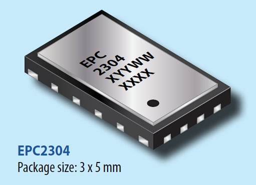
EPC2304 GaN FET in 3 x 5mm package. Image used courtesy of EPC
The new devices are pin compatible with the existing EPC2302, EPC2306, and EPC2308 100 V and 150 V, expanding EPCs FET to 200 V.
EPC claims that their GaN FETs are up to 15 times smaller with half the resistance of comparable silicon-based MOSFET solutions. The company further asserts that their new FETs offer the lowest resistance at 150 V and 200 V of any device in the market today.
In addition to lower resistances, when compared with silicon, GaN FETs also have lower gate and reverse recovery charge levels, which means fewer switching losses. Better efficiency at high switching frequencies allows for smaller passive components, which translates to more compact circuit designs in applications like switch mode power supplies (SMPS).
The new FETs are packaged in a 3mm x 5mm thermally enhanced QFN package. The packaging exposes the die to ambient and has a JDEC junction to ambient thermal resistance (ƟJA) of 45°C/W.
With a continuous current rating of ~ 100 A and a typical on resistance of ~ 3mΩ, the small package of the EPC2304 can theoretically accommodate continuous power levels approaching 30W, with proper thermal management in place.
The combined low conduction and switching losses and high power density make these FETs well-suited to applications like smaller and lighter BLDC motor drives and more compact and efficient DC-DC converters and solar optimizers, and microinverters.
Constructing a GaN FET
To help contain costs, EPC builds its GaN devices using depreciated, low-resolution CMOS foundries. The EPC process begins with a silicon wafer on which a thin Aluminum Nitride (AIN) layer is grown to isolate the transistor structure from the substrate. A highly resistive layer of GaN is then developed on top of the AIN. Aluminum is added to the GaN to help form a conductive depletion region under the Gate, and metal layers are added for the three transistor terminals. This structure is repeated multiple times to create the power FET.
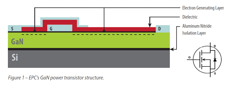
GaN power transistor structure. Image used courtesy of EPC
Lower On Resistances at High Voltage
Although relatively new, GaN devices have an important advantage over silicon and, even more recently, high-voltage silicon carbide compounds with respect to the theoretical trade-off between on resistance and withstand voltage. This means they can offer higher voltage ratings with lower conduction losses.
The distance between the drain and gate is increased to raise the voltage rating of a GaN device. Since the material's resistance within the depletion region of a GaN device is relatively low, these FETs can offer lower resistances, even at high voltage. By comparison, achieving a higher withstand voltage in silicon results in a greater penalty in terms of higher resistance, to the point that silicon MOSFETs are increasingly less practical in many higher voltage applications.

GaN offers better voltage and resistance trade-offs. Image used courtesy of EPC
Wide Bandgap Is a Characteristic, not a Feature
It’s important to note that wide bandgap is a characteristic of compounds like GaN, not a feature. GaN FETs and silicon carbide generally require more energy and higher gate voltages to induce conduction in their channels. This can add complexity to the surrounding drive circuitry compared to more conductive silicon.
Despite using older, depreciated foundry equipment, any special processing, packaging, and test requirements may have cost implications. The EPC2304 is priced at $5.25 per unit when purchased in volumes of 1,000.
Evaluation for Half-bridge Power Applications
The EPC90140 is an evaluation board and reference design with integrated drivers that employ the EPC2304 in a half-bridge power circuit that can be configured as a buck or boost converter.
The 2” x 2” board, along with reference schematic, BOM, and layout files, allows designers to quickly evaluate the FETs and can serve as a jumping-off point for new product development initiatives.

Functional schematic of EPC90140 development board. Image used courtesy of EPC

EPC90140 development board, Image used courtesy of EPC