Facebook
 Google
 GitHub
 Linkedin
Embedding Capacitors Into Interposers for Greater Miniaturization
A team of scientists from Tokyo Institute of Technology developed a 3D functional interposer that saves package area and allows for low noise and power consumption.
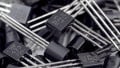
Today's electronic devices and computers consist of circuits with many millions of transistors. We can observe this trend in progress from SSI (Small-Scale Integration) devices containing tens of transistors to VLSI (Very Large-Scale Integration) devices with millions of transistors. This trend is fueled by a steady decrease in dimensions of the elements like transistors, interconnecting wires, etc. Currently, we are capable of making MOSFETs with lengths as small as a few nanometers. The dimensions of the interconnecting wires also reduced from tens of microns to tens of nanometers over time. However, this trend is bound to slow down as the materials and processes we implement reach their physical limitations.
Over the past decade, there has not been a significant amount of progress in the development of high-energy-density capacitors for VLSI devices. Generally, VLSI circuit designers try to avoid including capacitors in their design as they occupy a relatively large area. But they are crucial components in switched capacitor circuits, in pole-zero compensation for wide bandwidth circuits, for generating delays, for producing low-pass response, etc. Therefore, it is necessary to find clever ways for fabricating capacitors in less space while maintaining the actual capacity.
A team of scientists at the Tokyo Institute of Technology, led by Prof. Takayuki Ohba, has figured out a way to integrate capacitors inside the interposers. An interposer is an electrical interface providing vertical connections between the sockets or another chip. They demonstrated in their latest study, which will be presented at the 2021 IEEE Electronic Components and Technology Conference, that silicon interposers can be made into functional capacitors. This approach will save a considerable amount of space and present many more other benefits.
For low power consumption devices, a lower supply voltage is advantageous. Many low-power circuits today work with sub-1V supply voltage. Through testing and theoretical calculations, the scientists determined that their developed functional capacitors allowed for a wiring resistance of about 100 times lower than conventional designs, as well as lower parasitic capacitance. Thus, enabling the devices to work with lower supply voltages.
Embedding Capacitors into Interposers
Interposers are essential and very commonly used components in modern electronic ICs. 2.5D IC technology, also called interposer technology, combines multiple IC material dies in a single package. It is a halfway technology to 3D ICs, that incorporates MOS transistors manufactured by stacking silicon wafers vertically. In 2.5D ICs, the chips like RAMs and microprocessors are placed on top of interposers. As mentioned earlier, interposers are an electrical interface between the chip and the board. The dies are stacked side-by-side on top of an interposer, which incorporates through-silicon vias (TSVs). The use of interposers provides high bandwidth density and efficient energy utilization compared to other interfaces.
The capacitors in 2.5D packages are placed on the package substrate close to the components, but the connections still have to be made to the chip. This layout increases the package substrate area and causes layout problems like high wiring resistance and noise due to the interconnections needed.
The scientists at the Tokyo Institute of Technology directly embedded the silicon capacitors in the interposer, eliminating the need for interconnections. They embedded the capacitive elements inside a 300 mm silicon piece using permanent adhesive and mold resin. The connections between the chip and the capacitors are made with through-silicon vias without solder bumps.

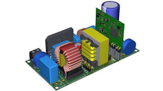
The new interposer design with an embedded capacitor. (Source)
In bumpless chip-on-wafer designs, the formation of warp due to resin and misplacement errors due to empty packets in the adhesive are the two common problems. The researchers, nevertheless, managed to avoid them.
"Our bumpless 3D functional interposer enables a notable reduction in package area of about 50% and an interconnect length a hundred times shorter,” Ohba said.
About the researchers
The team of scientists involved in this study is led by Dr. Takayuki Ohba. Dr. Takayuki Ohba is a Professor at Tokyo Institute of Technology (Tokyo Tech) from 2013 and The University of Tokyo from 2004 to 2013, respectively. His research focus is on production-worthy processes and co-integration to achieve ultra-small tera-scale devices without sacrificing power efficiency and cost.