Facebook
 Google
 GitHub
 Linkedin
Bidirectional Power Transistors for Battery Management Systems
Innoscience’s 100 V devices use GaN-on-silicon technology with bidirectional blocking capability.
Battery management systems (BMS) are integral to modern power systems. However, as power demands rise, especially in high-density applications like 48 V and 60 V battery setups, conventional silicon-based systems face efficiency, footprint, and cost challenges. As a result, semiconductor materials that can more effectively handle high-power, high-frequency requirements are in strong demand.
Innoscience has introduced a 100 V bidirectional gallium nitride-on-silicon (GaN-on-silicon) transistor designed to streamline BMS architectures and improve efficiency. The transistor could overcome many limitations of current BMS technology.
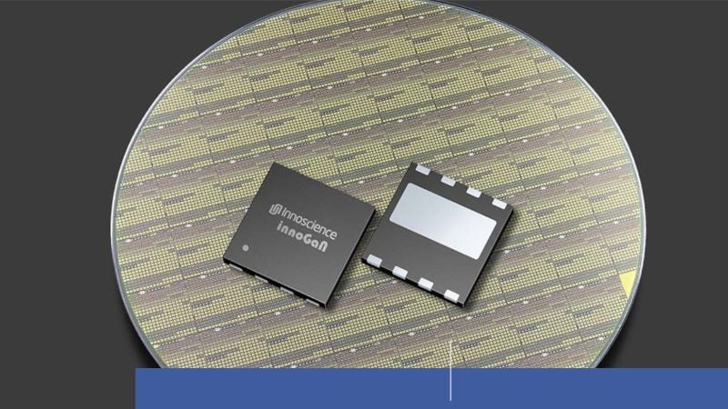
Innoscience GaN-on-silicon. Images used courtesy of Innoscience
The Battery Management System
Battery management systems are intelligent systems that optimize battery performance through continuous monitoring and precise control. By implementing sophisticated algorithms for charging and discharging cycles, they extend battery lifespan, provide accurate predictions of remaining battery life, and maintain optimal operational conditions.
However, as power demands rise, so do technical challenges in BMS design. Traditional BMS architectures typically rely on silicon MOSFETs to manage cell balancing, charging, and discharging processes. However, silicon-based MOSFETs exhibit inherent limitations that impact performance, especially under higher power conditions. The higher on-resistance in silicon MOSFETs results in greater conduction losses, which generate heat and ultimately lower the system's energy efficiency.
_1.jpg)
Battery management system schematic. Image used courtesy of Dimitrov et al.
Another challenge in traditional BMS architectures is achieving efficient bidirectional operation using silicon MOSFETs. A typical approach involves a back-to-back MOSFET configuration to enable current flow in both directions. In this setup, two MOSFETs are placed in series but oriented in opposite directions, allowing control over both charging and discharging paths. However, this arrangement introduces additional complexity and resistance, as each MOSFET contributes to the overall on-resistance. The added resistance limits current flow and generates extra heat, decreasing overall efficiency and often necessitating additional cooling components.
Innoscience’s INV100FQ030A
Innoscience has developed the INV100FQ030A, a 100 V voltage-rated bidirectional transistor for BMS architectures.
The solution is a GaN-on-silicon enhancement-mode device that achieves improved efficiency and performance. Compared to silicon solutions, GaN semiconductors have a wider bandgap (3.4 eV), which allows them to handle higher voltages and temperatures. At the same time, due to the material’s higher electron mobility supports, the devices exhibit decreased resistances to reduce conduction losses and offer faster switching speeds to minimize switching losses. The INV1000FQ030A transistor, for example, includes a dynamic on-resistance of just 3.2mΩ, packaged within a compact 4x6mm form factor.
Notably, the device eliminates the traditional requirement for dual back-to-back silicon MOSFETs thanks to a common-drain configuration that enables bi-directional switching capabilities. A bidirectional transistor supports multiple operational modes, including two-way pass-through, two-way cut-off, and no-reverse-recovery modes, enabling support for battery charging and discharging operations within a single component.
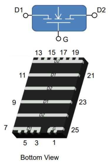
The symbol and package for INV100FQ030A. Image used courtesy of Innoscience
To improve safety, the device has four operational modes: standard charge and discharge, charge protection, discharge protection, and sleep mode. Available in En-FCQFN (exposed top-side cooling) and FCQFN packaging options, this device builds upon Innoscience's successful 40V VGaN series, already implemented in USB overvoltage protection systems for major smartphone manufacturers.
Overall, Innoscience says the device is best suited for applications requiring efficient power management, such as house batteries, portable charging stations, and electric mobility solutions like e-scooters and e-bikes.
Future Implications
As battery technology progresses, efficient power management solutions like Innoscience’s 100 V GaN-on-silicon transistor could pave the way for more streamlined, sustainable, and cost-effective designs in energy storage systems. By reducing the complexity and space required for bidirectional power flow, these transistors offer practical enhancements for BMS.
Related Content