Facebook
 Google
 GitHub
 Linkedin
1200V Reverse Conducting IGBT Optimized for Hard Switching
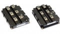
Fuji Electric has developed a 1200V reverse-conducting (RC) IGBT based on the company's latest thin wafer process. The 1200V RC-IGBT enables increased module ratings: upgrading a 1200V, 800A module to 1000A in a DualXT package and upgrading from 35A and 1200V in a small power integrated module (PIM) to 50A. At the same time, the reduced temperature ripple effect in power cycling improves the reliability of the modules.
The performance of this RC-IGBT shows the same relationship between conduction loss and switching loss as Fuji’s 6th generation conventional IGBT and FWD. In addition its trade-off can be optimized for hard switching by lifetime killer. Calculations of the hard switching inverter loss and chip junction temperature (Tj) show that the optimized RC-IGBT can handle 35% larger current density per chip area.
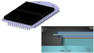
In order to utilize the high performance characteristics of the RC-IGBT, Fuji has developed a new compact package. This module can handle 58% higher current than conventional 100A modules at a 51% smaller footprint. In addition, the RC-IGBT chip was mounted in the newly-developed compact package that has low thermal impedance and high reliability. Advantages of the new package include:
(1) Compact; Conventional package uses Aluminum wire bonding and a circuit pattern on the DCB substrate for the connection between chips and terminals. These methods need a certain amount of area for the wire bonding and the circuit. In the new package, copper pins are used instead of wire bonding and a power connected board instead of a circuit pattern on the DCB substrate. Copper pins are soldered vertically on the chips and the power connected board is arranged just above the chips. This methodology eliminates space for wire bonding and circuit pattern on the DCB substrate. Consequently the footprint of our new package is less than half of conventional packages.
(2) Low thermal impedance; The new structure uses Si3N4 for insulating material, which thermal conductivity is less than half of conventional materials like Al2O3. In addition the new structure uses a thick copper plate on both sides of ceramic substrate. These copper plates effectively spread the heat from the chips to the cooling fin. As a result the thermal impedance of our new structure is less than half compared to conventional structure.
(3) High reliability; Regarding the reliability of this IGBT module, power cycling capability has the biggest impact. In the power cycling test, the wire bonding on the chip and the solder layer between chips and the DCB substrate are the weak points of the conventional structure. As explained above the new structure eliminates wire bonding by using copper pins thus the power cycling capability of the new package strongly depends on the solder layer lifetime. Epoxy resin is used as encapsulating material instead of silicone gel. In the power cycling test, epoxy resin causes the effect of thermal stress dispersion at the solder layer due to its rigidity. Consequently the concentration of thermal stress at the solder layer is greatly reduced which leads to long lifetime of the solder layer.
The module footprint of the new package is 51% less than that of the conventional package and the chip size of the downsized RC-IGBT is 26% smaller than that of the conventional IGBT and FWD. The Rth(jc) of the downsized RC-IGBT assembled in the new package is 62% lower than that of the conventional IGBT assembled in conventional package. Fuji believes that the combination of the RC-GBT and the revolutionary package is promising candidate for the downsizing of IGBT module and as a result complete inverter systems.